
CHAPTER FIVE
Electronic and Photonic Materials
CHAPTER SUMMARY
The Panel on Electronic and Photonic Materials was charged with examining materials research needs for future defense systems in electronics, optoelectronics and photonics, and microsystems (including sensor systems). The tremendous vitality and innovation of the private sector allowed the panel to consider which future defense needs could be met by making use of commercial developments in industry and which were so specific to DoD as to require DoD investment.
The panel began by examining the following military needs that would particularly benefit from advances in electronic and photonic materials:
-
Detection, identification, and defense against or avoidance of threats;
-
High-fidelity imaging signals;
-
Communications systems;
-
Compact systems to transmit at very high power and high frequency;
-
Enemy identification and monitoring;
-
Dynamic camouflage/stealth; and
-
Health monitoring of equipment and personnel.
While this panel considered a wide variety of military needs from several vantage points, ranging from individual devices or components to entire miniature systems, a number of common themes emerged that point to important areas for research:
-
Improvements in the fundamental understanding of existing materials that have been identified as promising for military applications;
-
The search for new materials with extreme properties, sometimes orders of magnitude better than what is currently available;
-
New ways of combining materials, particularly at the nanoscale, in order to obtain new functionality, with particular attention to ways to routinely combine inorganic and organic or even biological materials;
-
Consideration of packaging and thermal management issues, in parallel with research on materials for the devices themselves;
-
Materials processing to effect the successful introduction of new materials and the optimization and manufacturability of existing materials (low-temperature processes are generally desirable and sometimes essential, particularly as device dimensions shrink and as increasingly dissimilar materials are used in close proximity to one another); and
-
Theory and modeling as indispensable partners of experimental efforts in the search for and optimization of new materials, especially as nanoscale structure and control become paramount.
INTRODUCTION
The Panel on Electronic and Photonic Materials was charged with examining materials research needs for future DoD systems in three areas: (1) electronics; (2) optoelectronics and photonics; and (3) microsystems, including sensor systems. Progress in electronic and photonic materials and systems that are heavily dependent on them, such as microsystems and sensors, is occurring at an astonishing rate, fueled in large measure by tremendous investments by the private sector. This panel considered which future defense needs could be met by taking advantage of commercial developments and which were so specific to DoD as to require DoD investment. Each section of this chapter discusses (1) commercial drivers; (2) DoD drivers where materials have potentially high impact; and (3) priorities for DoD-funded materials research.
DOD NEEDS FOR ELECTRONIC AND PHOTONIC MATERIALS
The panel considered the following military needs, identified by DoD leaders,1 to be particularly ripe for resolution via advances in electronic and photonic materials:
-
Detection, identification, and defense against—or avoidance of—threats. Low-cost, highly capable commercial technologies are increasingly enabling even nations with very limited resources to mount considerable regional threats based on precision strikes from their own territories. This development, coupled with the periodic U.S. need to mount operations in a wide variety of conditions, requires increased reliance on systems that can detect, identify, defend against, or avoid many types of threats. Because such systems must be deployed on military equipment, as distributed sensors, or on individual soldiers, they must be compact, light, energy-efficient systems with broad capabilities.
-
High-fidelity imaging signals. Imaging systems that could be used to identify camouflaged soldiers and materiel by soldiers or on vehicles (manned or unmanned) would reduce casualties and materiel loss.
-
Compact systems to transmit at very high power and high frequency. Compact high-power systems would allow operation of communications and surveillance equipment at greater distances. Size and weight will determine whether such systems are appropriate for use on unmanned vehicles or by individual soldiers. Operation in new high-frequency regimes allows for higher bandwidth as well as access to spectroscopic information that is not accessible in other frequency ranges.
-
Communications systems. Increased coordination among forces, the need for global awareness, and increased reliance on information from remote sensors and unmanned vehicles all drive the need for compact, energy-efficient communications systems that can transmit and receive securely at high bandwidth.
-
Enemy identification and monitoring. Monitoring of enemy troop and materiel movement, as well as discrimination between enemy and friendly elements, will become increasingly important as future conflicts move to new battlefields, such as urban environments.
-
Dynamic camouflage/stealth. The ability to dynamically change the spectroscopic signature of surfaces, either on soldiers or equipment, would greatly reduce the probability of detection by the enemy.
-
Health monitoring of equipment and personnel. Monitoring of personnel for health or exposure to chemical or biological agents will become increasingly important. Monitoring the health of equipment in the field is also a longstanding need, as already detailed in Chapter 3.
SPECIFIC AREAS OF OPPORTUNITY
Below, DoD needs in three specific areas of opportunity are discussed: electronics, optoelectronics and photonics, and microsystems.
Electronics
Commercial Drivers
The silicon-based microelectronics industry has been a tremendous force in the U.S. economy for at least two decades. The phenomenal ability of the industry to keep pace with, and even exceed, Moore’s Law (doubling the logic density every 18 months, with a concomitant reduction in cost/bit) has put unprecedented data processing and storage in the hands of every American. The trend is expected to continue for another decade, as documented in the 2001 edition of the International Technology Roadmap for Semiconductors (ITRS) (SIA, 2001). DoD can leverage this revolution by taking advantage of industrial developments. For the longer term, the conclusion of the ITRS is that “10-15 years in the future, it becomes evident that most of the known technological capabilities will approach or have reached their limits.” It projects that a more cost-effective alternative to planar silicon complementary metal oxide semiconductor (CMOS) technology will be required in this time frame. The solution may involve new materials, new cell architectures, and new processes.
This forecast represents the first projection that scalable planar silicon CMOS is reaching a limit. Along with this singular discontinuity several
other critical material needs are identified in this roadmap for the commercial semiconductor segment over 10-15 years:
-
Mask materials and photoresists for <45-nm lithography,
-
Wafer materials and crystal-growing technology for >300-mm wafers (450 mm), and
-
Yield model development for new materials and integration.
DoD needs to support research into novel materials for nanoscale integration beyond the limits of CMOS scaling. The commercial sector is driving the increase in information storage capability at the same rate as Moore’s Law, although the relatively high level of DoD investment has enabled this industry to take advantage of new materials developments more aggressively than has happened for semiconductors.
DoD Drivers with Potentially High Materials Impact
During this century U.S. effectiveness in battle will depend on the superiority of our ability to gather information that allows us to identify, locate, and destroy or at least avoid the threat (see Figure 5-1). In spite of very rapid progress in electronic materials and systems, it has not been possible to keep up with the increasing demand for compactness, power (high or low, depending on the application), simplicity in packaging, and signal purity. Since many future military systems will be space based, use lighter platforms, or be deployed on individual soldiers, these demands are becoming imperatives. Significant improvement over existing capabilities can be achieved only by inserting novel high-performance electronic materials into sensors, detectors, and components.
The following military technologies are particularly ripe for improvement:
-
Detection, identification, and defense against—or avoidance of—threats,
-
Compact systems to transmit and receive very high or very low power at very high frequencies, and
-
Embedded technologies that enable these systems.
Certain components in these systems are in particular need of materials advances, including
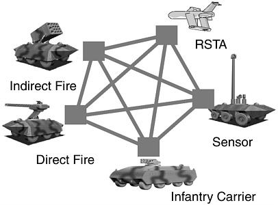
FIGURE 5-1
Relationships in the Future Combat System. SOURCE: Browning, V.M., “An Overview of Electronic Materials,” briefing presented to the Panel on Electronic and Photonic Materials of the Committee on Materials Research for Defense After Next, National Research Council, Washington, DC, March 29, 2001. RSTA = Reconnaissance, Surveillance, and Targeting Antenna.
-
Transmitters, receivers, and detectors for high-frequency broadband systems;
-
High-power electronic components;
-
Analog/digital converters;
-
Electronic beam steering;
-
Radio frequency (RF) microsystem components;
-
Acoustic components; and
-
Ferroelectric materials.
In addition, materials developments that are on the horizon or that may be envisioned could provide the basis for revolutionary technological advances; among them are superconducting materials and nanostructured materials.
Transmitters, Receivers, and Detectors for High-Frequency Broadband Systems The military needs materials for transmitters, receivers, and detectors that can operate at frequencies from MHz to over 100 GHz frequencies. SiGe is seen as the next-generation material for high-speed, high-frequency applications, but it is not suitable at the highest frequencies; these require different materials, most likely the group III-nitride crystals and their derivatives. Materials research should concern itself with developing appropriate substrates, optimizing epitaxial growth (which will require better understanding of fundamental aspects of the growth of these polar materials), and improving the junctions and contact layers (which will entail identifying important defects and ways to eliminate or control them).
High-Power Electronic Components The high-power transmitters and receivers in future systems cannot be made using traditional semiconductors like Si or GaAs. Materials for low-frequency and high-power applications like SiC and its derivatives are promising, but achieving the required signal purity must be rooted in a fundamental understanding of how to control their chemistry, crystal growth, epitaxy, and defect density.2 The group III-nitride materials are also promising, but meeting the operating requirements for high-power applications or in hostile ambients will require interconnects and overlayers that can function around 500°C. In addition to detailed understanding of crystal growth and the control of important defects in the materials, attention must be paid to high-temperature contact materials, overlayers, and joining materials. A hybrid of carbides and nitrides of gallium, aluminum, and boron is one promising approach, although the monumental challenges of design, fabrication, and processing are still to be solved.
Analog/Digital Converters Electronic analog-to-digital converters (ADC) have continued to show steady but slow progress in resolution and speed (Walden, 1999). Performance limiters due to sampling aperture jitter and comparator ambiguity are directly related to device speed; electronic materials that yield faster devices will accelerate progress. Optical ADC and optically assisted ADC have shown promise for improving perfor
mance but they need new materials with 500 times higher electro-optical coefficients than lithium niobate or other oxide materials. Preliminary experiments suggest that semiconductor materials like rubidium hydrogen selenate class materials, solid solutions, or substituted II-VI, II-VI materials have potential (Guilbert et al., 1998).
Electronic Beam Steering One of the biggest challenges facing defensive systems is replacement of the mechanical or optical (mirror) beam steering with all-electronic laser-beam steering. This could be achieved with materials whose damage threshold, modulation capabilities, and transparency properties are amenable to electronic steering. Tailoring the Bragg diffraction of materials is one promising approach. As a function of microwave frequency, the angle, power, and wavelength for steering could be controlled if a material with suitable diffraction characteristics could be produced.
RF Microsystem Components Microelectromechanical microwave switches have a wide range of applications in military systems. They have extremely low insertion loss (0.2 dB) and crosstalk over a broad microwave frequency range (>40 GHz). Microwave phase shifters based on MEMS RF switches have shown much lower insertion loss than conventional electronic phase shifters. This reduces the number of amplifiers needed and also the size, weight, and power of phased-array antenna systems. A MEMS RF switch could also be used in frequency agile filters. Materials affect the reliability of these switches. Engineering of metal electrodes with low contact resistance and no stiction during separation is critical for metal-to-metal contact switches, especially for hot switching under high-power conditions. Prevention of dielectric charge-up is essential for capacitive switches. RF MEMS components will also play an important role in future wireless communication systems, as discussed below.
Acoustic Components Improved materials are needed for space and underwater acoustics. The materials properties that are important are power capability, sensitivity, noise performance, size, weight, robustness, shock resilience, aging, manufacturability, cost, and bandwidth. Materials must meet stringent performance criteria, including high Q, low loss, and temperature-stable operation. Artificially structured ternary and quaternary materials are promising. Theory and modeling will be important in finding material solutions to the severe constraints of this problem.
Ferroelectric Materials Ferroelectric materials have high dielectric constant, wide tunability, or both. Unfortunately, current ferroelectrics are limited to low dielectric relaxation frequency. Ferroelectrics with much higher dielectric relaxation frequency would allow miniaturization and tunability of high-frequency microwave circuits.
New Materials For Tomorrow’s Technologies While high-transition-temperature materials have attracted most of the scientific interest in superconductivity in recent years, most commercial superconducting devices use lower transition-temperature materials composed only of metals. Industry has invested heavily in oxide superconductors for passive microwave components, SQUID magnetic-field sensors, high-current conductors for power transmission and high-field magnets, and Josephson-based circuits for mixed-signal (analog and digital) circuits and AC voltage standards. The recently discovered borides are also receiving considerable attention.
While superconducting materials offer potential performance advantages over conventional materials, this has so far come at the cost of additional system complexity due to both the refrigeration requirement and the challenges posed by other properties of the materials, such as the brittleness and anisotropy of high-temperature superconductors. Unless refrigeration becomes efficient and reliable or higher temperature superconducting materials are discovered, superconducting devices will be relegated to niche military applications.
Speculative concepts such as quantum devices and spintronics have the potential to dramatically change the way military information is processed and encrypted. These concepts require exquisite control of material structure and properties on the nanometer if not subnanometer scale—a tremendous growth and processing challenge. The development of materials in the form of arrays of nanowires instead of thin films is a promising approach. New materials may also be needed. While the risks of such research are high, the possible payoffs for the first nation to field systems based on the successful embodiment of some of these concepts may be immeasurable. In the limit of miniaturization, it can be expected that electronic devices will reach the scale of small numbers of atoms or molecules—the domain of molecular electronics. The challenges associated with realizing this dream are discussed in Chapter 6.
The military will continue to have an insatiable appetite for data storage. The sorts of materials issues that arise in pushing storage density
limit to the ultimate are essentially the same as for other nanostructured materials: the needs to control structure and composition on the atomic or nanometer scale, and to be able to read and write on that same scale. The specific materials required will also probably be different from today’s.
Priorities for DoD Materials Research in Electronic Materials
The priorities for DoD-funded research into electronic materials fall into only a few categories:
Fundamental Understanding of Existing Materials Known materials, such as SiC and Group III-nitrides, are very promising for high-power and high-frequency applications. These materials are different from and in many respects more complex than the materials they would replace. Understanding the performance limits of the materials, as well as achieving them reproducibly, will require a multipronged scientific investigation incorporating experiment, theory, and modeling.
New Materials with Extreme Properties The need for a material with an electro-optic coefficient 500 times higher than traditional oxides to meet new requirements for ADCs is an example of extreme materials properties that will require new approaches to materials structure and processing. The desire for electronic materials that can function around 500°C is also an extreme demand. Room-temperature superconducting materials and quantum devices would profoundly change system options. Theory and modeling will be key in guiding the experimental approaches to promising compositions and structures.
Packaging and Thermal Management High-power devices that may function at temperatures around 500°C place severe requirements on interconnect, overlayer, and packaging materials and on the system components in close proximity to the device itself.
Materials Processing Optimizing the performance of existing materials and successfully fabricating new ones with extreme properties will succeed or fail in large measure with the emphasis given first to understanding and then to controlling their fabrication and processing. As an example, improved materials and processing will enable production of components and subsystems (Figure 5-2) for frequency-agile communication and radar
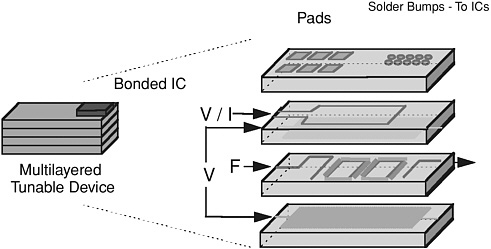
FIGURE 5-2
Generalized concept incorporating oscillators, filters, phase shifters, and circulators for a multilayer package with integrated circuits to improve quality and impedance matching. SOURCE: Courtesy of S. Wolf, DSO Office, DARPA.
applications that take advantage of the field-variable properties of ferroelectrics, ferrites, and other new materials.
Theory and Modeling Understanding the role of defects and the relative importance of defects in materials like SiC and GaN will depend heavily on theory. Elimination or control of the most detrimental defects is likely to be done experimentally, with significant guidance from growth models. In design of new materials with extreme properties, theory is likely to guide modelers to the most promising general structures and compositions. Modeling in turn will be required to narrow the list of most promising materials to a number that can be tested experimentally.
Materials for Revolutionary Technologies The scaling of both Si planar CMOS technology and high-density storage using known approaches will reach fundamental limits within the next 15 years. Perhaps the most fruitful area in which to look for potentially revolutionary technologies is in materials and material architectures that would enable entirely new approaches to computation, encryption, and data storage. A first step in this direction would be to find materials and processes that could be used to demonstrate experimentally some of the current theoretical concepts in
quantum computing, spintronics, etc. (Gupta et al., 2001; Roukes, 2001). Materials concepts that may be relevant are:
-
Integration of different functions on the nanometer or possibly atomic scale,
-
Parallel material architectures that enable parallel function or fault tolerance,
-
Self-assembly and self-repair, and
-
Reconfigurability.
The integration of carbon nanotubes or biological molecules into material structures to perform some or all of these functions is an intriguing possibility.
Conclusions
The might and productivity of the commercial sector in silicon technology and in magnetic and optical storage technology dictate that the DoD leverage this technology base as much as possible. DoD investments should emphasize electronic materials for systems to identify, locate, and engage or defend against threats; for compact systems to transmit very high power at very high frequencies; and for embedded technologies that enable these systems. Materials research investments that are most likely to pay dividends are fundamental studies to increase understanding of existing materials; development of new materials with extreme properties; materials processing; packaging and thermal management; theory and modeling; and materials for revolutionary technologies.
Optoelectronics and Photonics
Commercial Drivers
The primary commercial drivers for photonic and optoelectronic materials are telecommunications, data communications, high-speed interconnects, optical data storage, light-emitting diode (LED) lighting, displays, and instrumentation. Telecommunications focus on InP and related materials operating at wavelengths around 1.55 mm. Datacom emphasizes high-volume and low-cost manufacturing using GaAs and InP materials. High-speed interconnects among electronic systems, boards, and chips, or even within chips, employ arrays of low-cost lasers and detectors
using mainly GaAs-based materials, such as very short reach vertical cavity surface-emitting lasers. Heterogeneous integration on silicon substrates or organic substrates and even printed circuit boards is of interest to reduce cost and size. GaN and other wide-bandgap semiconductors are the main materials for optical data storage, LED lighting, and large panel display applications. There is no direct overlap between the commercial and DoD drivers in terms of materials.
DoD Drivers with Potentially High Materials Impact
The DoD drivers for future optoelectronic and photonic materials can be divided into three categories: (1) weapons, (2) electro-optic sensors, and (3) communications. The weapon applications include high-power lasers and infrared countermeasures (IRCM). Sensor applications include imaging at various bands from visible to very long infrared wavelengths, multispectral and hyperspectral imaging, terahertz imaging, laser radar, sensing of chemical and biological agents, and sensor/eye protection. In the communications area, DoD requires broadband coverage of RF signals with high fidelity. The material requirements for these applications are far beyond those of commercial drivers. The panel focuses its discussion on inorganic materials; organic photonic materials are discussed in Chapter 6.
High-Power Lasers Laser weapons require output power exceeding one kilowatt. Laser materials with high saturation power/fluence and high thermal and dielectric damage thresholds are key. Solid-state lasers are the main contenders for high-power lasers. For solid-state lasers, the primary challenge is the growth of large laser crystals with few defects or impurities.3 Most current efforts focus on the growth of pure bulk crystals. Artificially engineered laser materials could increase the size and spatially vary properties. One example is fusion bonding of individual crystals to form larger crystals with dopant concentration gradients for uniform heat deposition and spatial mode improvement (Machida et al., 1998). Another is ceramic media created by hot-pressing powders of conventional laser materials to form large rods with tailorable concentration (Jianren et al., 2001).
Infrared Countermeasures Infrared seekers use different detectors to observe the IR signature of aircraft. The IRCM laser must cover every potential detector wavelength band with sufficient power. Optical parametric oscillators (OPOs) can efficiently shift laser wavelengths through the mid-IR region. Broad wavelength tunability is possible. The challenges are to develop new materials with both high nonlinearity and large power handling capability. Phase matching is critical for high conversion efficiency. Quasi-phase-matching (QPM) using periodically modulated materials is a powerful technique to force phase matching (Burr et al., 1997; Finsterbusch et al., 2000).
Clever engineering of composites of known materials may produce the best new materials. Several QPM techniques have been proposed, including stacking crystals of alternating orientations, periodic poling of polymers or fused silica, ferroelectrics, asymmetric quantum wells, and epitaxial growth of semiconductor materials on template substrates. Engineering of the grating could further tailor the properties of synthetic nonlinear materials. For example, multiple gratings can be used for broad tuning of OPOs, with each grating designed for a different wavelength. Aperiodic gratings can shape ultrafast femtosecond pulses similar to digital filters.
Another challenge of IRCM is replacing optical steering mirrors with electronic beam steering (as discussed briefly above). Electronic switching could be achieved by using dielectrics, piezoelectrics, photoconductors, or semiconductors. This will require design and production of film and bulk hybrid materials with properties well beyond those of traditional oxides. Magnetic antennas, antennas that can steer and tailor radiation patterns dynamically, and periodic dielectric structures that forbid propagation of electromagnetic waves in a certain range require novel bulk and thin-film crystals. MEMS micromirrors and electro-optic beam steering devices are also promising.
Materials with high damage threshold, fast modulation capabilities, and low absorption are required. Materials for phase shifters with extremely low loss at high frequency are essential. This will require the design and fabrication of tunable materials with low-loss dielectric and piezoelectric properties. Materials scientists have to look beyond the horizon of traditional materials to multinary materials. Possible approaches are fabrication of crystalline materials with a large number of different atoms and huge unit cells, or the combination of more traditional materials integrated in one, two, or three dimensions on the nanometer or micrometer scale. The synthesis and processing of such complex materials will be a daunting challenge.
Focal Plane Arrays and Multi- and Hyperspectral Imaging Hyperspectral imaging (HSI) sensors in the reflective region of the spectrum (sometimes referred to as imaging spectrometers) acquire digital images in many contiguous and very narrow (nominally about 0.010 µm wide) spectral bands in the visible, near-IR, and mid-IR portions of the spectrum (0.4–2.5 µm). This enables the construction of an essentially continuous radiance spectrum for every pixel in the scene. Thus, HSI makes possible the remote identification of ground materials of interest based on their spectra signatures. HSI has great potential for identifying camouflaged soldiers, trucks, tankers, and other military vehicles. It would be particularly attractive if systems could be included in army vehicles as well as in the equipment of an individual soldier.
HSI complements and enhances radar imaging. Major materials challenges are focal plane arrays covering ultraviolet (UV), IR, and very long wavelength IR regions. Current IR focal plane arrays are based on selenide- and telluride-based materials or inter-subband transitions in quantum wells (Dyer and Tidrow, 1998; Gunapala et al., 2000).
The semiconducing bandgap of carbon nanotubes (sub-100 meV to a few hundred meV) and the ability to control bandgap through tube diameter and chirality make them attractive for IR detection in the 1-15 µm range (Xu, 2001). Tuning is achieved by varying nanotube diameter. The cylindrical symmetry of the nanotubes allows absorption of all linearly polarized light, so that increasing the film thickness (i.e., tube length in a well-aligned film) increases absorption in a carbon nanotube-based detector. The major materials challenge here is to consistently control the parameters that govern nanotube electrical properties.
Electro-optic sensors for information-gathering and battlefield operations present similar challenges. There is a dearth of materials to meet the requirements of such systems. Materials with large acousto-optic merit will need to be designed, fabricated, and processed, requiring significant interplay among theory, modeling, experiment, and engineering. For small systems it is essential to have materials and the concomitant processes and packaging that can operate at UV, mid-, and far-IR wavelengths. Warfighter camera-type systems can achieve much higher resolution and range if better materials for light-gathering and detection are identified and developed.
Eye/Sensor Protection Optical limiters protect sensors from strong laser irradiation. Passive optical limiters can use optical processes such as
absorption, refraction, or scattering. Materials with giant nonlinear optical properties are needed. Nonlinear photosensitive liquid crystals have been used in optical limiters (Khoo et al., 1998). Because the nonlinear optical coefficients scale inversely with the bandgap (to the third or fourth power), giant nonlinear effects in traditional bulk media are unlikely. Instead, nano-engineered materials are promising for increasing nonlinear effects. Nonlinear photonic crystals and nanostructured materials are also promising, as are metal-dielectric nanocomposites that can enhance the electrical field. Strong confinement of electrons in organic materials or quantum dots may lead to enhanced nonlinear optical coefficients. Porous sol-gel glasses with thermal index change could enhance nonlinear optical scattering. To protect the eyes of soldiers, the optical system needs to be lightweight and much less bulky. Nonlinear optical coatings would be ideal for this application. They would require an even larger (104!) enhancement of nonlinear optical properties and present tremendous materials challenges.
Terahertz Imaging The terahertz frequency range has many DoD applications (Mickan et al., 2000). The primary application is imaging, including satellite-to-ground. Terahertz radiation offers better resolution than millimeter waves and can detect covered targets (e.g., tanks under trees). It is also useful for detecting landmines, though it is limited to dry soil because water has high attenuation in the terahertz range. Terahertz radiation can image subsurface structures and is useful for airport security and medical diagnosis. Currently, the dominant techniques to generate terahertz radiation use optical rectification excited by femtosecond optical pulses. Optical rectification requires materials with large second-order nonlinearity. New materials such as nonlinear organic media or periodically poled lithium niobate and other artificially structured materials with enhanced efficiency are needed. On the receiver side, crystals with high nonlinearity, better phase matching between optical and terahertz waves, and low birefringence are needed.
Photomixing is another technique to generate terahertz waves whose frequency is equal to the difference frequency of two continuous-wave laser beams. High-efficiency and high-power photomixers are required. Materials such as low-temperature grown GaAs have been successful for short optical wavelength sources. New materials responding to long wavelengths (1.55 µm) could take advantage of rapid advances in commercial telecommunication technology. Ultimately, all-solid-state terahertz sources using inter-subband transitions in quantum wells, superlattices, or
other bandgap-engineered semiconductors would be the most compact and energy-efficient sources (Williams and Hu, 2001). Most semiconductors, however, have phonon bands in these wavelength regions (8.8 THz for GaAs, and 10.4 THz for InP). New “phonon-engineered” materials may have to be created for this technique to become practical.
Chemical/Biological Sensing Photonics will continue to be a primary approach to sensing chemical and biological agents in the form of gases, vapors, aerosols, or surface-bound media. For chemical sensing there are several different techniques. The main material challenges are for new IR laser media. Compact semiconductor quantum cascade lasers (QCLs) are a recent breakthrough that extends the wavelength range of semiconductor lasers well into the mid-IR. The lasing wavelength of the QCL can be tailored by bandgap engineering, but operation is currently limited to cryogenic temperatures. For biosensing, UV fluorescence will likely remain a predominant detection technique because of its sensitivity and ubiquity among biological species. The lack of efficient UV laser and detector media are barriers to progress. Wide-bandgap semiconductors made from GaN are receiving the greatest attention in the engineering research community, but fundamental studies are lacking. These issues are discussed further in the section on microsystems.
Communications Broadband RF photonic links and systems are needed for transporting and processing signals from RF sensors and phased-array radars and to transmit signals to towed decoys. These systems require high dynamic ranges and large signal-to-noise ratios. Commercial developers of fiber optic networks are primarily concerned with digital signals. The material challenges for DoD are broadband electro-optic (EO) materials with high EO coefficient and high optical power-handling capability. Current materials like bulk EO crystals and semiconductors are approaching their limit. New materials based on photonic crystals could greatly enhance modulation efficiency. Though EO polymers are promising for broadband operations because of close index matching between optical and microwaves, their temperature range is very limited (Steier et al., 2001). New EO polymers that are stable at higher temperatures are desired.
Priorities for DoD Research in Optoelectronic and Photonic Materials
As the above discussion makes clear, most innovations in materials lie in clever engineering of materials in the nanometer (1 to 100 nm) range (nano-engineered materials). Nano-engineering refers to combining two or
more different materials in one, two, or three dimensions. Nano-engineered materials encompass many different classes of materials, including photonic crystals, as shown in Figure 5-3 (dielectric/air or dielectric/metal at the 100-nm scale); electronic bandgap-engineered materials (one-dimensional semiconductor superlattices or heterostructures at 1- to 10-nm scales); quantum dots; nanowires; and many other novel materials. Combining these capabilities monolithically would enable realization of photonic and/or photonic/electronic device integration. Successful nano-engineering will depend critically on the guidance of theory and modeling to determine what structures should be made. Materials processing will then play a crucial role in fabricating reproducible structures with the required tolerances.
Photonic bandgap materials are promising for achieving significantly higher EO, nonlinear optical, and acousto-optic coefficients than bulk materials. These materials will affect many DoD applications, including IRCM, sensor/eye protection, and RF photonic communications. They promise to enhance the sensitivity of detectors over a specified wavelength range, which will have an impact on multispectral and hyperspectral imaging. They can also be used for IR camouflage of soldiers. Achieving the same level of control over photons in photonic bandgap materials that we currently take for granted for electrons and holes in semiconductors will require the teamwork of theorists, modelers, and experimentalists. Achieving photonic bandgap structures in all the wavelength regions of interest will be a grand challenge for materials processing.
Electronic bandgap engineering can tailor the electronic and optical properties of materials. It extends the wavelength coverage of lasers and detectors over that of conventional bulk or quantum well materials. QCLs extend the laser wavelength into the VLWIR region. IR detectors, focal plane arrays, and hyperspectral imaging could benefit from type II semiconductors or bandgap-engineered materials.
In addition to DoD encouraging nano-engineered materials, continued support for discovering new host materials is also important. These include semiconductor materials with larger bandgap (for UV lasers/detectors) and small bandgap (infrared focal plane array) and photonic materials with large EO, nonlinear optical, and acousto-optic coefficients for nonlinear and EO applications.
Heterogeneous materials at the microscale (1 to 100 µm) are important for photonic materials. Large laser crystals with tailorable dopant gradients can be formed by fusion bonding of individual crystals with different
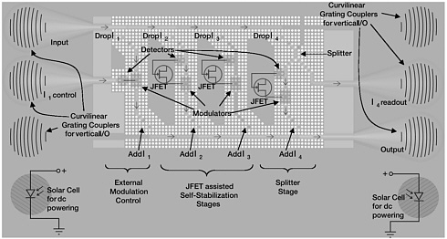
FIGURE 5-3
Schematic of nanoscopic photonic integrated circuits made of photonic crystals. Note that four WDM channels are shown, but that is meant to be representative of many more channels per chip. SOURCE: Courtesy of E. Yablonovitch, University of California, Los Angeles.
doping concentrations. Novel techniques to synthesize quasi-phase-matched materials will be useful for high-efficiency nonlinear materials.
Organic materials have improved tremendously in recent years in the variety of functions they can perform and in their aging and reliability characteristics. As discussed in Chapter 6, organic materials are likely to play a role (either alone or in concert with other materials) in achieving at least some of the functionality described here. The materials research needs for organic materials for optoelectronic and photonic applications is in many respects similar to the needs described here for inorganic materials.
In addition to the potentially revolutionary technologies discussed, such as photonic bandgap engineering, other concepts such as optical computing are very exciting but will depend to a large degree on advances in materials for their realization.
Conclusions
The major DoD drivers for future optoelectronic and photonic materials are for weapons, EO sensors, and communications. There is no direct overlap of materials needs between commercial and DoD drivers. While continual progress could be made by improving current materials, greater opportunities lie in nano-engineered materials with tailorable optical or EO properties. These include photonic bandgap materials, electronic bandgap-engineered materials, nanocomposites, and quasi-phase-matched materials. These materials are the most promising route to improving performance by orders of magnitude, as DoD applications require. In order for these materials to be exploited to the fullest, close collaboration between theorists, modelers, and experimentalists will be essential. Control of the structure and properties of materials on the nanoscale will present a tremendous challenge for materials processing.
Microsystems
Commercial Drivers
Microsystems and MEMS are subjects of continuing R&D; commercial products are established and new applications are emerging. Arrays of steerable micromirrors, for example, are used in computer projector systems and are available for optical communications and other applications. Accelerometers for triggering the deployment of automobile air bags are now based on MEMS technology, as are commercial ink-jet printers. A variety of simple “lab-on-a-chip” devices are commercially available, and new concepts for chemical analysis, drug discovery, medical diagnostic and other uses are being explored. Commercial development of environmental chemical sensing systems will be vigorous, second only to medical sensing in projected private efforts. Food-related sensing efforts are targeting mainly microbial agents that cause spoilage, with some attention to genetically modified organisms. Both will stimulate commercialization of sensing systems with features similar to those needed for military purposes: small systems targeted at a few specific species in a matrix of many other (dissimilar) species. However, specifications for analysis times, target analytes, and reliability that are unique to military applications will require a separate effort.
Commercial microsystems technology is at a relatively early stage; unlike in microelectronics, there are no established material or technology
platforms. Current microsystems materials include silicon-based materials, polymers, and ceramics. Much of the technology now being exploited in the commercial sector was supported initially by DoD and other federal funding. Significant R&D efforts are also in Europe, Japan, and other foreign countries. Because the costs are very high, and the risks significant, it is unlikely that U.S. industry alone will be the major driver for new materials and technology. DoD has an opportunity to play a significant role here, both to meet its own needs and to enhance U.S. competitiveness in this important but infant technology.
DoD Drivers with Potentially High Materials Impact
Microsystems that comprise electronic or photonic devices integrated with structures and devices that expand functionality beyond data transmission and processing are beginning to show clear promise as a revolutionary technology. During the next 20 to 30 years, they will become increasingly important for a wide range of defense applications. Microsystems may incorporate MEMS and microoptoelectromechanical systems (MOEMSs). With advances in materials processing, nano-electromechanical systems (NEMSs) may be created that include new device behaviors that capitalize on their small size, reaching ultimately to the molecular scale.
Miniaturization and integration of complex functionality into microsystems will significantly improve performance compared to similar functions performed by existing macrosystems. Among the improvements, expected to be commensurate with the degree of miniaturization, are increased operating speed and ruggedness coupled with reduced power consumption and weight. Capabilities currently impossible in large-scale systems may be possible with microsystems, for example, ultrasensitive sensors or methods of displaying three-dimensional optical images by manipulating the complex reflectivity of surfaces with subwavelength resolution.
DoD will have an increasing need to rapidly identify and contradict a more diffuse and technologically varying class of threats to both civilians and combatants. Microsystems will be essential in counteracting such threats. Several drivers were considered in evaluating the DoD priorities for microsystems. The first is the creation with microsystems of distributed self-contained systems that sense, think, act, and communicate, to be widely distributed in fixed locations or readily carried by nontechnical civilian responders, soldiers, autonomous movable platforms, or piloted vehicles. A related driver is the need for rapidly collecting and communicating infor-
mation on human activity and the environment. A third driver addresses the unique military defense needs for information security and identification. A fourth driver is the need to maintain the health and performance of defense personnel and equipment. These drivers have led us to consider the following applications where microsystems could contribute significantly to defense capabilities:
-
Miniature mobile or distributed sensing capability;
-
Rapid biometric identification of individuals;
-
Security and encryption (e.g. locks, codes, and identification);
-
Soldier health monitoring and remote medical diagnosis and treatment;
-
Equipment monitoring, diagnosis, and failure prediction and analysis (see Chapter 3, the Structural Materials Panel report, for discussion of related issues);
-
Dynamic camouflage, stealth, and altered electromagnetic signatures;
-
High-density data storage and displays; and
-
Miniaturized chemical processing: power generation, propulsion, and point-of-use materials fabrication.
Inherent in the microsystems approach is the demand that function be integrated into a self-contained unit. Such a system would include, for example, not only a sensor or detector but also a method for sampling from a solid, liquid, or gas as well as a power source and a method for processing, storing, and transmitting information. Advanced systems could be capable of directed motion and intelligent response to a threat, such as location and identification of a chemical source and initiation of countermeasures.
The small volume and broad functionality of integrated microsystems will require new combinations of material properties and new processing methods. Future military microsystems are likely to incorporate diverse materials, bringing to the fore issues of interfaces and materials compatibility. Such integration will pose similar challenges as methods of materials processing and fabrication of reduced dimension devices evolve. While silicon processing technology is mature enough for production of inte-grated electronic circuits, manufacturing complex integrated devices with additional functionality will require more diverse materials and processing methods. Military technologies are likely to advance in concert with
advances in consumer products. For both applications, reduced cost and wider availablility of high-functionality systems are driving work on microsystems. Military applications will create new materials requirements, such as system lifetime or range of operating environments.
Microsystems will enable interaction with the environment in a variety of ways, coupled with information storage, processing, and communications. The panel envisions a class of devices that incorporates advanced electronic and photonic capabilities, such as high-speed data processing, laser/optical detection, and communication with other functions involving motion, material flow, chemical interaction, force transduction, and mass detection. General microsystem applications and enabling technologies include:
-
High-sensitivity sensors (physical, chemical, and biological);
-
Actuators for motion;
-
Transduction and measurement of small forces and masses;
-
Fluid control, including control of gas, liquid, and solid particulates;
-
Optical systems for detection, modulation, beam steering, displays, and information processing;
-
Data storage and processing;
-
Custom or combinatorial materials synthesis; and
-
Power generation.
The panel evaluated the potential for exploiting these capabilities for defense applications, with particular attention to areas of possible revolutionary enhancement of performance.
Materials engineered at the nanoscale may provide new properties to be exploited and used in microsystems, for example in ultra-high-sensitivity systems for detecting a broad spectrum of environmental parameters. Insight and inspiration can be obtained from emulating biological systems that have successfully attained the type of integration that the panel contemplates. Living creatures (some snakes, for example) have integrated highly sensitive sensors in an efficiently powered mobile unit that can not only detect IR signals but also analyze them and respond. Insects can detect trace compounds in the air or on a surface, follow the chemical trail to the source, and respond in appropriate ways, such as mating, laying eggs, or eating. Analogies to the functions we would like to emulate in artificial systems are evident.
Microsystems will rely on integration of power sources, such as harvesting ambient light or stored chemical or electrical power. Detectors and sensors will be integrated with electronic data storage and processing. Responses will be communicated to other units and human systems through electronic and photonic means.
Actuators for Motion MEMS, NEMS, and microsystems can move physical objects with dimensions from micrometers to the molecular scale. Moving components at the scale of hundreds of micrometers and below can be made by microfabrication processes based on lithography, etching, and deposition. These structures can be moved by electrostatic, thermal, or magnetic drive. The motion of these devices, possibly at high frequency or by the contact of material interfaces, raises issues of material wear, defect motion, and fatigue. In such small systems, mechanical properties and mechanical losses can be strongly influenced by surface effects or the inclusion and location of grain boundaries and defects. The fact that mechanical properties of materials may differ at the microscale must be considered in selecting materials for micro- and nanoscale systems. Molecules that generate motion, possibly extracted from or inspired by biological systems, are candidates for actuation of fine-scale motion.
Transduction and Measurement of Small Forces and Masses The converse effect to the actuation of motion and mass transport is the detection of motion, small forces, and mass. The forces on micro- and nanostructured materials can be detected by a variety of physical processes, such as the creation of a voltage on a piezoelectric material. Small changes in mass can be sensed by observing the resonant frequency shift of micro-oscillators. Modulated electron tunneling and deflection of a laser beam by a moving structure have also been used to detect small motions. Such approaches are used in commercial scanning probe microscopes, often using microfabricated cantilevers as the force or motion transduction elements. The optical, electrical, and piezoelectric—in addition to the mechanical—properties can be important for microstructures used in force transduction. Materials that can perform these functions must be integrated with other materials of different functionality.
Physical Sensors The transduction mechanisms mentioned above can be used to detect a variety of forces and physical properties of the environment. Miniaturized pressure sensors, based on measuring the deflection of a membrane, exist. Fluid flow can similarly be measured by detecting the
forces imparted to a moving device in contact with a moving fluid. Magnetic fields can be detected in a variety of ways, including measuring the deflection of a mechanical cantilever incorporating a magnetic thin film. Accelerometers and gyroscopes can be realized in microsystems where the linear and angular acceleration can be measured as the force on a movable mass.
Chemical Sensors The large variety of possible target analytes and ambients (see Table 5-1) demands microsensor systems that can manipulate and modulate samples physically, chemically, and spatially and probe several aspects of their structure simultaneously or in rapid succession. Stand-alone vapor sensors, sensor arrays, or even instruments with single-parameter detection elements can screen for a few recognized threats but cannot meet ultimate performance demands. These call for systems in which pretreatment and separation functions play an integral role. Combining spectral detection with pretreatment is a common theme in most state-of-the art chem/bio microsystem development efforts (Frye-Mason et al., 2000; Rowe-Taitt et al., 2000; Xu et al., 2000; Eiceman et al., 2001; Hocker, 2001; Wise et al., 2001) and should remain central to future efforts. Future systems will require reductions in size, analysis time, detection limits, and power. Enhanced sample capture, pretreatment, analysis, identification, and quantification will require incorporation of innovative materials or combinations of materials into systems using micromachining and related MEMS, MOEMS, or NEMS technologies.
The design and selection of the sensor interface materials that interact with the target analytes are critically important. A rational approach to probing independent features of analyte structure by means of monolithic or integrated heteroarrays is of utmost importance. Fundamental interaction models are needed to guide the design of such multitransducer interface materials. Linear-solvation-energy-relationship (LSER) models (Grate, 2000; Hierlemann et al., 2001) provide an excellent example of a broadly applicable modeling paradigm. The tradeoffs between selectivity, reversibility, and stability of molecular recognition interactions (Hierlemann et al., 1999) must be recognized and incorporated into materials development strategies.
Polymers will figure prominently in future chemical sensing systems as sensor interface layers as well as for preconcentration adsorbents, separation membranes or phases, fluidic components, and perhaps even substrates. Rationally designed and synthesized polymeric sensor interfaces for
TABLE 5-1 Microsystems for (Bio)chemical Targets
|
Application |
Description |
Reference |
|
Chemical warfare agent monitoring |
Detection of nonbiological species; known nerve, blister, blood toxicants; environmental concentrations; personal-sphere concentrations; airborne as gas or vapor; aerosol-adsorbed; waterborne; surface-borne; sensing battlefield environments |
SBCCOMa |
|
Biological warfare agent monitoring |
Detection of pathogenic organisms; viral, bacterial, fungal; environmental concentrations; personal-sphere concentrations; airborne as free or adsorbed aerosol; waterborne; surface-borne; battlefield environment sensing |
Walt and Franz (2000), NIJb |
|
Explosives detection |
Detection of landmines, water mines; direct detection of explosive chemicals; surrogate measures (package material, physical presence) |
Dubey et al. (1999) |
|
Combat identification |
Chemical markers to discriminate friendly soldiers; enemies (previously tagged) |
NRC (2001) |
|
Trigger for protective measures |
Alarm level for deploying/donning/doffing (automated) personal protective equipment; antidote administration |
Armyc |
|
Dose monitoring |
Measurement of biological fluids (internally or externally) to assess extent of internal exposure or physiologic effect of exogenous agents; trigger for protective measures or antidotes; early warning of adverse health effects |
NRC (2001) |
|
Enemy presence |
Gas, vapor, aerosol composition signatures indicative of personnel or mechanized troop presence |
SBCCOMa |
|
Fire warning |
Early warning of damage to vehicles, quarters, aircraft |
Rose-Pehrsson et al. (2000) |
|
Wound status |
Early indicators of infection |
NRC (2001) |
|
Nuclear non-proliferation |
Detection of byproducts of nuclear weapons production |
CMCd |
|
aSBCCOM. 2001. Soldier and Biological Chemical Command. Available online at <http://www2.sbccom.army.mil/hld/>. Accessed June 26, 2001. bNIJ, National Institute of Justice. Available online at <http://www.ojp.usdoj.gov/nij/pubs.htm>. Accessed December, 2001. cArmy. 2001. U.S. Army Soldier Systems Center. Available online at <http://www.natick.army.mil/>. Accessed June 27, 2001. dCMC. 2002. Cooperative Monitoring Center. Available online at <http://www.cmc.sandia.gov/>. Accessed January 29, 2002. |
||
nerve agents (Grate et al., 1997; Levitsky et al., 2001) and explosives (Yang and Swager, 1998; Walt and Franz, 2000) have already yielded significant improvements in detection. These could serve as starting points for constrained combinatorial syntheses for further optimization.
Nanoscale device fabrication raises intriguing possibilities for new sensing modes. Nearly all current microsensing approaches rely on changes that occur within interfacial films over relatively long distances or that involve bulk phenomena. As interface domains shrink to the nanoscale and as measurements of interactions between discrete entities (e.g., single polymer strands and “a few” molecules) become analytically accessible, new sensing paradigms arise. Sensitivity and selectivity are likely to increase, although the magnitude remains to be seen. Control of temperature and other external variables will become even more important. This domain, now largely uncharted, may provide an opportunity for revolutionary advances.
Optical Sensors An alternative, complementary, detection strategy for chemical analysis is vibrational spectrometry. IR spectrometry in particular is capable of particle-density determinations, multicomponent vapor analysis, and structural identification. Emergent detection schemes include differential absorption LIDAR, frequency modulation spectroscopy, and heterodyne detection. Raman spectroscopy has similar capabilities. The inherent low sensitivity of IR absorbance by probed samples could be addressed by improvements in broadband/multiband IR sources, uncooled detectors, and optical pathlength enhancements or sample preconcentration (or other amplification schemes), as discussed below.
Microbolometer detectors, configured into focal-plane arrays (FPA), possibly as micromachined dense arrays (Tezcan et al., 1999), appear to be a viable near-term approach to IR sensing in the wavelength regions of interest (mainly 2-5 µm and 8-12 µm and secondarily 1.5-1.8 µm and 2.0-2.4 µm). Particularly useful would be thin-film CMOS-compatible materials with high-temperature coefficients of resistance that improve upon known materials and that can be patterned on suspended bolometer structures.
A broadband IR source with wavelength selection or a source providing several discrete critical wavelength emissions compatible with spatially resolved FPA detection would enable IR spectroscopy with low detection limits. Compact IR semiconductor lasers are needed—for example, the long-wavelength QCL. Increasing the operating temperature for higher
power output would make miniaturized IR spectophotometry possible. Two-dimensional IR methods employing multiple-frequency modulations and heterodyne detection are just emerging. With proper temperature control, they could permit unprecedented analysis of structural features. Path length or other concentration enhancements will be necessary for a microspectrometer to be effective for detection of trace (i.e., sub-ppm) analytes by IR spectroscopy. As an example, surface-enhanced Raman spectroscopy (SERS) realizes increases in sensitivity of several orders of magnitude (Stokes et al., 1999; Sylvia et al., 2000).
Biological Sensors DoD needs sensors for biological agents and pollutants. State-of-the-art bioaerosol sensing arrays, based on immunochemical or polymerase chain reaction (PCR)-amplified DNA-fragment fluorometry, have similar limitations as well as false positives, reliance on reagents, and time-consuming sample-handling and assay procedures (Walt and Franz, 2000). Bacteria, viruses, and many bacterial toxins, as well as all known nutrient media for biological agents, have strong UV fluorescence spectra that can serve as signatures for remote biodetection. Efficient UV laser and detector media are largely materials limited. GaN-based wide-bandgap semiconductors are promising for blue and UV lasers, although a fundamental understanding of the material is still lacking. The lack of a lattice-matched substrate presents a challenge for epitaxial growth of high-quality crystals.
Specific biological sensing operates as a lock-and-key system where a set of intermolecular interactions is defined by the geometry of a receptor site and a complex target molecule. Recent studies of cell-surface interactions have shown that short peptide sequences can be specifically recognized. Likewise, supramolecular chemistry is now showing that several hydrogen bonds between two molecules of constrained geometry are sufficient for a strong and specific bonding interaction. Such interactions are readily accessible in solution-phase systems but less so in gas-solid systems.
Many synthetic sensing systems are based on immobilized antigens or antibodies where binding is detected because of a mass change or other physical effect. Many sensors are also based on immobilized enzymes, which can be used to determine the concentration of substrate through pH change or redox reaction. A number of research directions are appropriate for developing specific sensors. Molecular modeling of intermolecular interactions is needed to enable the design of specific binding systems, to
make a lock for any given key, and to define the necessary properties for a specifically detectable key.
Biosensors will require materials and assembly processes for thermal and fluid support systems for living cells. In addition, these sensors will need to be processed monolithically with the rest of the microsystem (Table 5-1). The biological aspects of these challenges are discussed in the report of the National Research Council Committee on Opportunities in Biotechnology for Future Army Applications (NRC, 2001).
Sensor Response Amplification Through Material Property Transitions Amplification forms a complementary theme for interface material development, as discussed in the Bioinspired and Bioderived Materials report (Chapter 7). While there are many biological examples, nonbiological amplification mechanisms also deserve attention. The realignment and reorientation of liquid-crystalline (LC) domains due to the interaction of an analyte with the anchoring site of an immobilized LC is a good example of this phenomenon (Shah and Abbott, 2001). Large changes in optical (and probably other) properties occur due to the long-range reorientation in a material caused by a single interaction site disruption. Another example is the use of photonic-lattice diffraction gratings with vapochromic materials (Bailey and Hupp, 2002), where refractive index changes are selectively enhanced by orders of magnitude near the visible-light absorption maxima of the interface material. Changes in polymer modulus contribute significantly to surface-acoustic-wave (SAW) sensor responses, calling for design of polymers that capitalize on this feature to enhance sensitivity (Grate and Zellers, 2000). Similarly, thickness-shear-mode (TSM) and SAW sensors can reach resonance conditions where responses become discontinuous, a possible source of an order-of-magnitude increase in response. Operating near phase transitions or conduction percolation thresholds represents other sources of response amplification. Nano-engineered materials with so-called hard (rigid) and soft (flexible) regions are an attractive option for designing in such properties. Guidance from theory and modeling will be essential.
Sample Manipulation, Fluid Control, and Thermal Management Microsystems for chemical and biological sensors or reactors (see below) require the transport and manipulation of fluids. Preconcentration, chemical reaction, and separation will generally require
active mass transport. In liquid-phase systems employing aqueous media, this can be achieved with voltage biases at various points in a system. Gas systems relying on suction- or pressure-driven mass transport using microscale diaphragm pumps are being considered for microsystem applications but scale unfavorably with miniaturization.4 The flexural-plate-wave approach (Moroney et al., 1991; Meng et al., 2000), whereby gas flow could be achieved by acoustic streaming, has been suggested but not fully explored. Distributed transport mechanisms based on ciliary, peristaltic, or other biomimetic actuation could be options for gas transport. Efficient low-power valves and pumps for both gas and liquids require chemically inert thin-film materials.
Preconcentration and focusing of samples, perhaps selectively, can be achieved with porous materials of adjustable surface area, pore size, and functionality. Common but proprietary materials used for this purpose are carbon molecular sieves, graphitized carbons, and rigid polymers, which are thermally stable to over 400°C. Adapting these or similar types of materials, to allow in situ deposition, patterning, and control of porosity within etched channels of a microsystem would be useful for gas-phase and liquid-phase analysis. Tailored organic/inorganic nanocomposites are an attractive class of nanoengineered materials for this application. Templating by incorporation of porogens of selected sizes or functionality can impart a crude level of selectivity in these supramolecular systems (Raman et al., 1996).
Molecular separation based on controlled motion, competitive binding, or affinity would also benefit from nanoengineered materials and micromachined channels. Imparting structural features that would allow modulation of the binding or affinity with electric or photonic input would be a novel means of providing in situ control of separations. Clever channel construction methods and architectures that build upon anisotropically etched Si (Matzke et al., 1998), vapor-phase deposited polymers,5 and sacrificial-polymer processing (Mastrangelo et al., 1998; Bhusari et al., 2001) are examples of current research. Hybrid organic-inorganic nanocomposites are also promising (Lu et al., 2001).
|
4 |
Cabuz, C. 2001. Available online at <http://www.darpa.mil/dso/thrust/md/Mm/pump/honeywell/html>. Accessed March 29, 2001. |
|
5 |
Noh, H.-S., C. Bonner, P.J. Hesketh, and G.C. Frye-Mason, “Fabrication of Parylene Column for Micro Gas Chromatograph,” paper presented at the International Symposium on Mechatronics, Atlanta, GA, 2000. |
Finally, heating and cooling elements are needed to control the temperature of certain systems components. Microfluidic systems may provide thermal management. Alternatively, thermoelectric (TE) materials offer a promising approach. Unfortunately, thermal desorption and temperature-programmed separations require heating and cooling rates and values that exceed the capabilities of current TE materials. Materials or approaches that reduce demands for high temperature or that allow high temperatures to be achieved at low power are required. Fluid motion could also be used for control of the optical or mechanical properties of devices.
Other Novel Applications Important R&D activity is under way on MEMS devices and microsystems for optical devices, data processing, data storage, and displays, motivated by both defense and consumer applications such as telecommunications. MEMS-based systems for chemical and biological sensing are also being pursued vigorously.
With the opportunities to develop new sensor and actuator microsystems come significant materials challenges. The same types of fluid control systems being developed for sensors may also be exploited in microsystems for controlled chemical reactions. These chemical reactor systems could be used to generate power, for example, through internal combustion or fuel-cell-type reactions. These power sources could integrate with microsystems or be used for other compact power applications, as discussed in Chapter 4. Miniaturized or highly parallel chemical reaction systems could also be used for combinatorial approaches to fabricating novel materials for study or for creating materials that might be difficult or impossible to fabricate in bulk. Highly miniaturized reaction systems even approaching the nanoscale may provide a path to effective nanomaterials fabrication and processing, a need identified in Chapter 6.
Priorities for DoD Materials Research on Microsystems
The panel envisions microsystems with more diverse materials than current electronic, photonic, sensor, or structural systems. Materials for signal processing, power transmission, and communication will need to be integrated with materials that provide structural, chemical, or mechanical functions. Compatibilities among diverse materials, particularly at interfaces, will be increasingly challenging. As component dimensions shrink and nanoscale materials are employed, surface/volume and interface/ volume ratios will be large. Methods to interface nanoscale (grown)
materials with engineered devices will grow in importance. Issues like thermal expansion mismatch and interdiffusion must be mitigated.
Exploitation of nanoscale phenomena and even connection of biological or bioderived materials may be a valuable direction, because biological systems have arrived at solutions to many of the functionality issues we hope to address. The effective incorporation of bioderived or bioinspired materials into durable engineered systems remains a challenge. Nanoscale elements, perhaps carbon nanotubes, or functional macromolecules with nanoengineered properties may provide new material options. This raises the need to integrate molecular components into functional systems.
One of the fundamental areas for significant research will be on compatible materials for the control, metering, and flow of fluids. The panel envisions mass flow control with capabilities resembling those of electrical charge and light-flow control in electronic and photonic systems. Similarly important will be the ability to actuate and detect the motion of mechanical components in fluid and dirty environments. Chemical resistance and compatibility are likely to be critical, and there is strong motivation to incorporate into integrated systems materials with broad chemical resistance. Thermal management and temperature stability will also be important.
Fabrication of Microsystems In fabricating microsystems, one can build on the processes already well developed for microelectronic and photonic device and substrate fabrication. Lithographic processes created for the semiconductor industry can be exploited with the addition of etching and growth processes specific to the broader range of microsystem materials. Hybrid arrays of discrete sensors have been reported (Haug et al., 1993) and even commercialized (Gardener and Bartlett, 1999), but have not yet been fully exploited. With the possible exception of acoustic-wave sensors requiring a piezoelectric transduction layer, current sensor substrate materials are not performance-limiting. Furthermore, they are compatible with CMOS processing (Hagleitner et al., 2001), permitting integration of heteroarray sensors with each other and with Si-based circuitry and MEMS components. Such a monolithically integrated heteroarray could provide a wide variety of sensors with electronics and a full range of MEMS capability, but fabricating such a complex microsystem presents tremendous materials processing challenges.
The capability of controlling the location of polymers with different properties within microscopic tolerances throughout a microsystem needs
to be developed for microanalytical systems. In situ thermal or photopolymerization from liquid- or, preferably, gas-phase precursors is one promising approach (Healey et al., 1995; Prucker et al., 1999; Hsieh and Zellers, 2002; Yu et al., 2001). Nanometer-resolution soft lithography (Huck et al., 2001), laser-induced manipulation and deposition of nanoscale particles (Niidome et al., 2001), and matrix-assisted laser desorption (Pique et al., 2000) are other novel approaches. Further technique developments and the design of materials for deposition, patterning, in situ modification, and adhesion could yield significant payoffs.
Microsystem Packaging The packaging of electronics continues to be an area demanding new materials. For microelectronics, the drive to higher densities, higher speeds, and smaller sizes increases the need for thermal management. Military devices and sensor-based microsystems may be required to operate in hostile environments, placing even greater demands on electronics packaging. Materials are needed that are mechanically durable, thermally stable, and impervious to gas or chemicals that could alter the devices. The packages must also allow for low-loss electrical connections. Photonic devices must connect to guided-wave or free-space optics, requiring materials with transparency across various parts of the electromagnetic spectrum. Sensor-based microsystems create additional demands on materials; they must be nonmagnetic, chemically inert, and even biocompatible. These microsystems also require interconnections for mass transport and storage of biochemical materials. Low-temperature processing and joining methods must be developed that are compatible with the new materials. The demand for new materials and processes for electronic, photonic, and microsystem packaging is very strong; lack of appropriate materials may limit the functionality of future systems.
DoD will need packaging methods that allow for systems to interact with the environment in ways—e.g., exchanging fluids, chemical communication, and optical coupling—that protect components that are environmentally sensitive. Packaging must also be robust, enabling device operation in environments as hostile as inside a human body, an operating engine, or a high-speed vehicle.
Conclusions
Microsystems are already showing their promise as a revolutionary technology that gives future U.S. military a significant advantage. The advantages of creating low-power, compact, lightweight, reliable systems
for defense applications are compelling. They motivate addressing the significant materials issues involved. Although substantial R&D activity is under way, attention is particularly needed to materials processing, incorporation of bioderived and bioinspired components, materials compatibility, integration of nanoscale materials with engineered devices, and packaging. In the near term, emphasis is likely to be on integrating known materials into microsystems in a way that preserves the functionality of each material. In the future, new materials will be needed to increase system functionality. Power and thermal management are critical crosscutting issues, with ultimate links to the materials used in electronic and photonic engineered systems. Mass flow control and chemical compatibility are emerging needs for many microsystem applications.
Rationally designed polymeric, nanocomposite, and anisotropic materials assembled or implemented in a way that allows response amplification, show significant promise as chemical microsensor interface materials and as preconcentration and separation media. Models to guide the design of such materials for multisensor heteroarrays are needed to optimize their information yield. Nanoscale devices that rely on quantum effects represent the most intriguing and potentially revolutionary avenues for research, with likely improvements in detection sensitivity and some promise for improved selectivity. Coupling materials design, synthesis, and film deposition strategies with MEMS and MOEMS device and system fabrication strategies is essential to mass production and to ensuring compatibilities during bonding, interconnecting, and packaging.
RESEARCH AND DEVELOPMENT PRIORITIES
This panel considered a wide variety of military needs from several vantage points, ranging from individual devices or components to entire (miniature) systems. Six common themes emerged that point to the most important areas of research.
Fundamental Understanding of Existing Materials
Important properties of many materials that are promising for defense applications are not well understood. While empirical engineering of known materials for a specific application can be expected to gradually advance the state of these materials, this approach has limits. The most
dangerous possibility, perhaps, is that an undiscovered intrinsic property of a material may ultimately make it wholly unsuitable for the application. On a more optimistic note, fundamental scientific understanding is likely to give knowledge of the ultimate properties of a material and serve as a guide to its optimal processing. Truly fundamental understanding of complex real-world materials is only possible through a judicious combination of experiment, theory, and modeling, with intense feedback among the three. This will become even more important as we explore materials on the nanoscale at the interface between the discrete (quantum) and continuum (bulk) regimes of material behavior, where widely applicable modeling tools have not yet been developed.
New Materials with Extreme Properties
The increased functionality integrated into ever-decreasing volume drives the search for new materials that have properties (e.g., nonlinear optical properties) that are enhanced by an order of magnitude or more over known materials. Comparable improvements in material purity are also likely to be needed. Nanoengineered materials whose structure, composition, and morphology are varied on a nanometer scale in one, two, or all three dimensions are probably required.
Another approach that is appropriate in some cases is to search for single-phase materials with more elements and crystallographic complexity than have historically been considered. Identifying such promising materials is daunting. Effective and efficient experimentation will require theoretical and especially computational tools that can deal with such complex systems reliably. Optimization and exquisite control of processing will be essential to the reproducibility of such complex structures, especially those that combine different classes of materials (e.g., organic and inorganic).
New Ways of Combining Materials
Another way of increasing functionality in a small volume is to combine materials in new ways. Routine incorporation of nanoengineered components into a system (especially a microsystem) would both add functionality and reduce volume and weight.
Different classes of materials need to be combined in ways that are only beginning to be studied. These combinations often use inorganic
materials that have high processing temperatures, structural rigidity, and known long-term stability with organic or even biological materials that have low temperature tolerances, relatively poor structural stability, sensitivity to the ambient (which is usually why they were chosen in the first place), and poor or unknown long-term stability. Processing such hybrid structures presents a tremendous challenge. The interfaces between materials must be understood, because the functionality often is derived from materials properties very close to the interface. As device and system dimensions shrink, interfaces become even more dominant because an increasingly higher percentage of atoms or molecules find themselves at one interface or another. Theory and modeling can be expected to serve as guides to selecting appropriate combinations of materials and processing methods.
Packaging and Thermal Management
Electronic and photonic materials will be integrated at increasingly greater scales in the coming decades. While the functionality that such systems provide will be staggering by today’s standards, it comes at a price. Packaging and thermal management will be a significant challenge. Research in these areas needs to be done hand in hand with research in the areas already outlined.
Materials Processing
Before they can be introduced into new systems, it will be necessary to understand, optimize, and control the processing of the materials discussed in this chapter. Fabricating such complex materials in the first place will be a formidable challenge, as will be the design of processes to incorporate these new materials into structures and devices for military systems. Low-temperature processes are desirable in most cases, indispensable in some.
The complexity contemplated is too great to be able to rely on empirical process optimization alone. Processing models built on a solid theoretical underpinning will be key. These models will need to span length scales from nanometers to the scale of the device.
Theory and Modeling
Every materials research need discussed in this chapter points to the critical role that theory and modeling will play. These tools are not, however, currently sufficiently advanced to provide what is needed. The linking of theory, modeling, and experiment in each paragraph above illustrates the need for all three to be advanced in concert over the coming decade. One essential is bridging the length scales, ranging from the nanoscale on which many of these materials will be structured to at least the device scale. It will also be critical to span time scales, from the times at which the materials respond (as short as picoseconds) to the length of time the material is expected to be deployed (years). This is truly a grand challenge to materials science.
REFERENCES
Bailey, R.C., and J.T. Hupp. 2002. Large-scale resonance amplification of optical sensing of volatile compounds with chemoresponsive visible-region diffraction gratings. J. Am. Chem. Soc.124(23):6767-6774.
Bhusari, D., H.A. Reed, M. Wedlake, A. Padovani, A.A. Bidstrup-Allen, and P.A. Kohl. 2001. Fabrication of air-channel structures for microfluidic, microelectromechanical, and microelectronic applications. Journal of Microelectromechanical Systems 10(3):400-408.
Burr, K.C., C.L. Tang, M.A. Arbore, and M.M. Fejer. 1997. Broadly tunable mid-infrared femtosecond optical parametric oscillator using all-solid-state-pumped periodically poled lithium niobate. Optics Letters 22(19):1458-1460.
CMC (Cooperative Monitoring Center), Sandia National Laboratories. Undated. Available online at <http://www.cmc.sandia.gov/>. Accessed December 11, 2001.
Dubey, A.C., J.F. Harvey, J.T. Broach, and R.E. Dugan, eds. 1999. Detection and Remediation of Mines and Minelike Targets IV. Bellingham, WA: SPIE.
Dyer, W.R., and M.Z. Tidrow. 1998. Applications of MCT and QWIP to ballistic missile defense. Proceedings of the SPIE—The International Society for Optical Engineering (Infrared Detectors and Focal Plane Arrays V, Orlando, FL, 14-17 April 1998). SPIE-Int. Soc. Opt. Eng.3379:434-440.
Eiceman, G.A., E.G. Nazarov, J.E. Rodriguez, and J.A. Stone. 2001. Analysis of a drift tube at ambient pressure: Models and precise measurements in ion mobility spectrometry. Rev. Sci. Instrum.72:3610-3621.
Finsterbusch, K., R. Urschel, and H. Zacharias. 2000. Fourier-transform-limited, high-power picosecond optical parametric oscillator based on periodically poled lithium niobate. Applied Physics B (Lasers and Optics) B70(6):741-746.
Frye-Mason, G., R. Kottenstette, P. Lewis, E. Heller, R. Manginell, D. Adkins, G. Dulleck, D. Martinez, D. Sasaki, C. Mowry, C. Matzke, and L. Anderson. 2000. Hand-held miniature chemical analysis system (µChemLab) for detection of trace concentrations of gas-phase analytes. Pp. 229-232 in Proceedings on Micro Total Analysis Systems 2000, A. van den Berg , W. Olthuis, and P. Bergveld, eds. Dordrecht, The Netherlands: Kluwer.
Gardener, W., and P.N. Bartlett. 1999. Electronic Noises: Principles and Applications. Oxford, UK: Oxford University Press.
Grate, J.W. 2000. Acoustic wave microsensor arrays for vapor sensing. Chemical Reviews 100:2627-2648.
Grate, J.W., and E.T. Zellers. 2000. The fractional free volume of the sorbed vapor in modeling the viscoelastic contribution to polymer-coated surface acoustic wave vapor sensor responses. Anal. Chem 72:2861-2868.
Grate, J.W., S.N. Kaganove, S.J. Patrash, R. Craig, and M. Bliss. 1997. Hybrid organic/ inorganic copolymers with strongly hydrogen-bond acidic properties for acoustic wave and optical sensors. Chemistry of Materials 9:1201-1207.
Guilbert, L., J.P. Salvestrini, P. Kolata, F.X. Abrial, M.D. Fontana, and Z. Czapla. 1998. Optical characteristics of triclinic rubidium hydrogen selenate. Journal of the Optical Society of America B—Optical Physics 15(3):1009-1016.
Gunapala, S.D., S.V. Bandara, A. Singh, J.K. Liu, B. Rafol, E.M. Luong, J.M. Mumolo, N.Q. Tran, D.Z.-Y. Ting, J.D. Vincent, C.A. Shott, J. Long, and P.D. LeVan. 2000. 640x486 long-wavelength two-color GaAs/AlGaAs quantum well infrared photodetector (QWIP) focal plane array camera. IEEE Transactions on Electron Devices 47(5):963-971.
Gupta, J.A., R. Knobel, N. Samarth, and D.D. Awschalom. 2001. Ultrafast manipulation of electron spin coherence. Science 292(5526):2458.
Hagleitner, C., A. Hierlemann, C. Lange, A. Kummer, N. Kerness, O. Brand, and H. Baltes. 2001. Smart single-chip gas sensor microsystem. Nature 414(6861):293-296.
Haug, K., D. Schierbaum, G. Gauglitz, and W. Gopel. 1993. Chemical sensors based upon polysiloxanes: Comparison between optical, quartz microbalance, calorimetric, and capacitance sensors. Sensors and Actuators B11:383-391.
Healey, S., E. Foran, and D.R. Walt. 1995. Photodeposition of micrometer-scale polymer patterns on optical imaging fibers. Science 269:1078-1080.
Hierlemann, A., A.J. Ricco, K. Bodenhoffer, and W. Gopel. 1999. Effective use of molecular recognition in gas sensing: Results from acoustic wave and in situ FTIR measurements. Anal. Chem. 71:3022-3035.
Hierlemann, A., E.T. Zellers, and A.J. Ricco. 2001. Use of linear solvation energy relationships to model acoustic wave vapor sensor responses. Anal. Chem. 73:3458-3466.
Hocker, B. 2001. The polychrometer: A MEMS-based optical correlation spectrometer. Available online at <www.darpa.mil/mto/mems/summaries/Projects/individual_32.html>. Accessed November 10, 2001.
Hsieh, M.D., and E.T. Zellers. 2002. In situ UV-photopolymerization of gas phase monomers for microanalytical system applications. Sensors and Actuators B82(2-3):287-296.
Huck, W.T.S., A.D. Stroock, and G.M. Whitesides. 2001. Synthesis of geometrically well defined, molecularly thin polymer films. Angew. Chem. Int. Ed. Engl. 39(6):1058-1065.
Jianren L., T. Murai, K. Takaichi, T. Uematsu, K. Misawa, M. Prabhu, J. Xu, K. Ueda, H. Yagi, T. Yanagitani, A.A. Kaminskii, and A. Kudryashov. 2001. 72 W Nd:Y3Al5O12 ceramic laser. Applied Physics Letters 78(23):3586-3588.
Khoo, L.C., B.D. Guenther, Min-Yi Shih, P.H. Chen, and M.V. Wood. 1998. Optical limiting of submicrowatt long-pulse cw lasers with extremely nonlinear nematic liquid crystal films. Pp. 374-375 in Technical Digest: Conference on Lasers and Electro-Optics, San Francisco, CA. Washington, DC: Optical Society of America.
Levitsky, I., S.G. Krivoshlykov, and J.W. Grate. 2001. Rational design of a nile red/polymer composite film for fluorescence sensing of organophosphonate vapors using hydrogen-bond acidic polymers. Anal. Chem. 73:3441-3448.
Lu, Y., Y. Yang, A. Sellinger, M. Lu, J. Huang, H. Fan, R. Haddad, G. Lopez, A.R. Burns, D.Y. Sasaki, J. Shelnutt, and C.J. Brinker. 2001. Self-assembly of mesoscopically ordered chromatic polydiacetylene/silica nanocomposites. Nature410(6831):913.
Machida, H., N. Iehisa, and N. Karube. 1998. 2.5 kW slab Nd:YAG laser using a 400 mm-long crystal bonded by optical contact method. Proceedings of the SPIE—The International Society for Optical Engineering (Laser Processing of Materials and Industrial Applications II, Beijing, China, September 16-19, 1998). SPIE-Int. Soc. Opt. Eng. 3550:469-476.
Mastrangelo, C.M., M.A. Burns, and D.T. Burke. 1998. Microfabricated devices for genetic diagnostics. Proc. IEEE86:1769-1787.
Matzke, C.M., R. Kottenstette, S.A. Casalnuovo, G.C. Frye-Mason, M.L. Hudson, D.Y. Sasaki, R.P. Manginell, and C.C. Wong. 1998. Microfabricated silicon gas chromatographic micro-channels: Fabrication and performance. Pp. 262-268 in Proceedings of the 1998 SPIE Conference on Micromachining and Microfabrication Process Technology IV, September, Santa Clara, CA. Bellingham, WA: SPIE
Meng, A.H., N.-T. Nguyen, and R.M. White. 2000. Focused flow micropump using ultrasonic flexural plate waves. Biomedical Microdevices2(3):169-174.
Mickan, S., D. Abbott, J. Munch, X.-C. Zhang, and T. Van Doorn. 2000. Analysis of system trade-offs for terahertz imaging. Microelectronics Journal31(7):503-514.
Moroney, R.M., R.M. White, and R.T. Howe. 1991. Microtransport induced by ultrasonic lamb waves. Appl. Phys. Lett.59:774-776.
Niidome, Y., A. Hori, H. Takahashi, Y. Goto, and S. Yamada. 2001. Laser-induced deposition of gold nanoparticles onto glass substrates in cyclohexane. Nano Letters1:365-369.
NIJ (National Institute of Justice). National Institute of Justice Publications. Undated. Available online at <http://www.ojp.usdoj.gov/nij/pubs.htm>. Accessed December 12, 2001.
NRC (National Research Council). 2001. Opportunities in Biotechnology for Future Army Applications. Washington, DC: National Academy Press.
Pique, A., D.B. Chrisey, J.M. Fitzgerald, R.A. McGill, R.C.Y. Auyeung, H.D. Wu, V. Nguyen, S. Lakeou, R. Chung, and M. Duignan. 2000. Direct writing of electronic and sensor materials using a laser transfer technique. J. Mater. Res.15:1872-1875.
Prucker, O., C.A. Naumann, J. Ruhe, W. Knoll, and C.W. Frank. 1999. Photochemical attachment of polymer films to solid surfaces via monolayers of benzophenone derivatives. J. Am. Chem. Soc.121:8766-8770.
Raman, N.K., M.T. Anderson, and C.J. Brinker. 1996. Template-based approaches to the preparation of nanoporous silicas. Chem. Mater.8:1682-1701.
Rose-Pehrsson, S.L., R.E. Shaffer, S.J. Hart, F.W. Frederick, D.T. Gottuk, B.D. Strhlen, and S.A. Hill. 2000. Multi-criteria fire detection systems using a probabilistic neural network. Sensor Actuator B69(3):325-335.
Roukes, M.2001. Electronic in a spin. Nature411(6839):747.
Rowe-Taitt, C.A., J.W. Hazzard, K.E. Hoffman, J.J. Cras, J.P. Golden, and F.S. Ligler. 2000. Simultaneous detection of six biohazardous agents using a planar waveguide array biosensor . Biosensors and Bioelectronics15:579-589.
SBCCOM (Soldier and Biological Chemical Command). Undated. Available online at <http://www.sbccom.apgea.army.mil/>. Accessed September 16, 2002; Homeland Defense. March 6, 2002. Available online at <http://hld.sbccom.army.mil/>. Accessed September 16, 2002; Defense Threat Reduction Agency. Undated. Available at <http://www.dtra.mil/>. Accessed September 16, 2002.
Semiconductor Industry Association (SIA). 2001. The International Technology Roadmap for Semiconductors, San Jose, CA. Available online at <http://public.itrs.net/Files/2001ITRS/Home.htm>. Accessed March 3, 2002.
Shah, R.R., and N.L. Abbott. 2001. Principles or measurement of chemical exposure based on recognition-driven anchoring transitions in liquid crystals. Science 293(5533):1296-1299.
Steier, W.H., M.-C. Oh, H. Zhang, A. Szep, L.R. Dalton, C. Zhang, H.R. Fetterman, D.H. Chang, H. Erlig, and B. Tsap. 2001. Recent advances in low voltage, high frequency polymer electro-optic modulators. Pp. 1-3 in OFC 2001: Optical Fiber Communication Conference, Anaheim, CA.
Stokes, D.L., A. Pal, V.A. Narayanan, and T. Vo-Dinh. 1999. Evaluation of a chemical vapor dosimeter using polymer-coated SERS substrates. Analyt. Chim. Acta 399(3):265-274.
Sylvia, J.M., J.A. Janni, J.D. Klein, and K.M. Spencer. 2000. Surface enhanced Raman detection of 2,4-dinitrotoluene impurity vapor as a marker to locate landmines. Anal. Chem.72:5834-5840.
Tezcan, D.S., F. Kocer, and T. Akin. 1999. An uncooled microbolometer infrared detector in any standard CMOS technology. Pp. 610-613 in International Conference on Solid-State Sensors and Actuators (Transducers ’99), Sendai, Japan, M. Esashi, ed. Tokyo: IEEE.
Walden, R.H. 1999. Analog-to-digital converter survey and analysis. IEEE Journal on Selected Areas in Communications 17:539-550.
Walt, D.R., and D.R. Franz. 2000. Biological warfare detection. Anal. Chem. Vol. 739A-746A.
Williams, B.S., and Qing Hu. 2001. Optimized energy separation for phonon scattering in three-level terahertz intersubband lasers. Journal of Applied Physics 90(11):5504-5511.
Wise, K.D., K. Najafi, D.M. Aslam, R.B. Brown, J.M. Giachino, L.C. McAfee, C.T.-C. Nguyen, R.O. Warrington, and E.T. Zellers. 2001. Wireless integrated microsystems (WIMS): The coming revolution in the remote gathering of information. Technical Digest for SensorsExpo Conference, Chicago, IL.
Xu, J., W.B. Whitten, and J.M. Ramsey. 2000. Space charge effects on resolution in a miniature ion mobility spectrometer. Anal. Chem. 72:5787-5791.
Xu, J.M. 2001. Highly ordered carbon nanotubes arrays and IR detection. Infrared Physics and Technology 42:485-491.
Yang, J.-S., and T.M. Swager. 1998. Fluorescent porous polymer films as TNT chemosensors: Electronic and structural effects. J. Am. Chem. Soc. 120:11864-11873.
Yu, M., H. Davey, F. Svec, and J.M.J. Frechet. 2001. Monolithic porous polymer for on-chip solid-phase extraction and preconcentration prepared by photoinitiated in situ polymerization with a microfluidic device. Anal. Chem 73(21):5088-5096.


