
1
Context and Overview
INTRODUCTION
Work in the chemical sciences on new materials offers many diverse opportunities; to detail all of them in a brief overview would be impossible. A few examples of technical challenges indicate the breadth of work in the chemical sciences on materials science and technology, particularly how these challenges relate to the need for interdisciplinary approaches between the chemical sciences and a number of other fields. These challenges should be viewed in a global, social context to perceive the full dimensions faced in meeting them.
TECHNICAL CHALLENGES
To define opportunities in the chemical sciences related to materials, it is necessary to determine where current scientific interest lies and what impact existing research and development has had on society. Three areas of great interest to the majority of scientists include bio-, information-, and nanotechnology. Although research in each of these fields has already offered great advances, remarkable opportunities remain for the discovery and application of new technologies.
Researchers in the chemical sciences form and manipulate materials at the atomic and molecular level. From this point of view, many modern materials are merely chemicals that have been “engineered” for use. Thus, for many materials, the differentiation between materials science and chemistry is blurred in a similar fashion to the manner in which chemistry and biology for many applications has become blurred (in the development of pharmaceuticals, for example).
Interfaces between the chemical sciences and other fields are always interesting, especially when these fields are experiencing explosive growth. Biology and information are two areas that interface with the chemical sciences, and should lead to exciting breakthroughs. Developments at the interface between engineered and nonbiological systems are anticipated in the long term. However, advances in the short term have been seen already. The broad goal of engineering the surfaces of materials to interface with biological systems, has led to breakthroughs such as the Dacron™ heart patch, the heart valve, and the tricuspid valve. Other advances in this area include the use of materials for replacement joints and new fabrics for tissue growth, including artificial skin. All of these advances have led to significant improvements in the quality of life for many patients. In addition, these advances often reduce costs and environmental impact.
Advances in information technology center on smaller semiconductor features. These features are now approaching the molecular scale in size. Thus, exquisite control of materials properties is required to impact areas such as information storage technologies (Sidebar 1.1), consumer electronics (Sidebar 1.2), or quantum computing. To accomplish this requires better preparation of both new and existing materials. A multitude of materials will be needed for these applications.
For example, polymer synthesis is being applied in the drive to reduce feature size. Biopolymers and biomimetic polymers have several materials properties of interest. These materials have applications in the design and construction of nanoscale integrated circuits, laminated structural elements (smart sensor interiors in automobiles, planes, and trains), and in microsensors that can be embedded in persons or animals or placed on protective clothing.1 (Advances in polymerization often rely on mimicking nature, increasing functionality, broadening particle size, and simplifying processes. The importance of this approach is reflected in the major effort at present in living free-radical polymerizations. See Sidebar 1.3).
Dielectric materials are used to insulate the microscopic wires between transistors on a chip. Materials with increasingly lower dielectric constants (k < 2) are needed to increase transmission for electronic devices that are becoming increasingly smaller and closer together. Polymer dielectrics have been an important advance for these applications. An important advance in the future may also be found using porous polymers.
Other opportunities exist in the area of nanotechnology. Carbon nanotubes
|
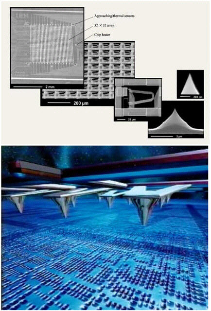
SIDEBAR 1.1 Information Storage Technologya There is an apparently insatiable demand for increasing microelectronic performance and storage capacity. Storage capacity has doubled roughly every three to four months. However, in traditional magnetics technology, physical limitations of the bit size used for data storage are rapidly being reached. As a result, new technologies are necessary. A novel project at IBM, the Millipede Project, addresses future ultra-high-density storage devices by using a thermal mechanical read-write strategy. This project uses an Atomic Force Microscope (AFM) based industrial-scientific-medical (ISM) band chip, which contains individual heated cantilevers (Figure 1.1). Contact of the heated cantilever tip with a thin polymer film produces a nanoscopic indentation or hole that can represent a bit of information (see Figure). Although potentially simple, if a single cantilever is used, an extremely slow read-write process results. Increased speed can be achieved by employing numerous AFM-ISM cantilevers in a highly parallel design, with each cantilever individually addressable. Using this technology, researchers have developed a 32 by 32 array of thermally heated AFM-ISM tips, yielding a total of 1,024 tips. Since each AFM-ISM tip operates independently, highly efficient and fast read-write operations can be achieved—hence the name Millipede. A problem still remains, however, with the polymeric recording layer. A very thin film is required of which little is known about the behavior, stability of the nanometer-sized bits, and the underlying principles of the writing and erasing process. All of these fundamental materials questions are critically important since a useful operating device would require the ability to read and write repeatedly. |
have received much attention due to their favorable electrical properties and strength. These materials may be thought of as rolled up sheets of graphite that can have different helical structures and can be singlewalled or multiwalled. It is difficult to predict the application of carbon nanotubes because of the current difficulty in reproducibly synthesizing and working with them. This may ultimately make silicon nanowires a more important technology. One area of particular difficulty is using nanotubes for electronic devices. Ideally, carbon nanotubes are unique, low-dimensional conductors with either metallic or semiconducting properties. In practice, however, these hollow cylinders have a strong tendency to agglomerate as they form, resulting in either large, multiwalled
|
SIDEBAR 1.2 Fundamental Technology Innovations: Replacement for the Barcodea The barcode has become so ubiquitous in our consumer society that many overlook its impact. Since it came into common use roughly 20 years ago, the barcode has been added to such a large array of products that it is difficult to find an item that does not carry a code. As useful as this system is, it does present some drawbacks. In a checkout line, the product barcodes are scanned serially. While this system is a vast improvement over manual entry of prices, it essentially still remains an advance of the earlier system. A fundamental change in the way items are purchased would be to eliminate this serial system at the end and replace it with a serial selection performed while the customer is shopping. With this system, the customer would simply select items that would then be tallied as he or she shopped. One possible innovation would be the development of a device that stores the information that is present on the barcode. This device could be powered externally through a small antenna. The actual circuit, which serves to store the barcode data, might have at least 10,000 transistors and a clock rate on the order of a kilohertz. The true innovation would be in the nature of this device. The replacement for the barcode would contain no silicon and would operate using polymer-based organics. Production would be by printing rather than by photolithography, and the cost would be less than one cent per copy. The nature of this device and its mode of production would lead to its manufacture on a massive scale. Already, the production of transistors in the United States is on the order of 39 per second. Production of a printed organic polymer device would be expected to surpass this rate. |
nanotubes with many concentric carbon shells or bundles (ropes) of aligned singlewalled nanotubes. Both aggregates are complex composite conductors incorporating many weakly coupled nanotubes, each having a different electronic structure. This complexity remains the primary difficulty in both understanding and developing nanotube-based electronic devices.2 Regardless, work on these
|
SIDEBAR 1.3 Tailored Macromolecules and Nanoscopic Materials: Polymers and Free-Radical Processesa Polymerization has traditionally been difficult to control. Living free-radical polymerization, which combines the best of traditional living polymerization and ionic chemistry, shows promise of changing this.b In living free-radical processes, a mediating radical sits at the end of a polymer chain. This chain is then activated by an external stimulus such as heat or the presence of a transition-metal catalyst. This can add a few monomer units. The mediator then returns and regenerates the dormant polymer chain. This process has increased the degree of polymerization by a limited number of monomer units, and the procedure can cycle, resulting in controlled growth of the polymer chain. The mediator is absolutely critical. It is involved in every step of the polymerization. Its structure will determine to a great extent what polymerizations are possible. Using high-throughput methods, it is possible to screen many initiators of catalysts rapidly. The beauty of these systems is that they are compatible with a wide range of different monomers and functional groups. Therefore, polymer size can be controlled from very low molecular weights up to more than a hundred thousand. Polymer shape can also be controlled. Living free-radical polymerization is an elegant example of the transfer of organic chemistry to the polymer community. |
types of materials requires new vapor, liquid, and solid catalytic reactions. These new classes of chemical reactions will open the door to fundamentally new kinds of materials.
The last 50 years have been described as the period of electronics, with the next 50 years expected to be the period of photonics. Information will travel and be stored using light (photons) rather than electrons. One of the major benefits in a change to photonics would be vastly increased bandwidth compared to electronic transmission. Bandwidth is the width of the range of frequencies that a signal occupies on a given transmission medium. Because the frequency of visible energy is so high (on the order of millions of megahertz), thousands or mil
lions of signals can be impressed onto a single beam by means of frequency division multiplexing. In addition, a single strand of fiber can carry visible light at several different wavelengths, each beam having its own set of modulating signals. The opportunities in this area are simply enormous.
Just as semiconductors exclude electron propagation for certain energy bands and thus allow for the construction of circuits, photonic band gap materials— crystalline structures that exclude light transmission in all directions for specific wavelength ranges—are being developed in an attempt to build so-called circuits of light.3 Photonic band gap materials are engineered three-dimensional diffraction gratings with interesting properties. An example would be a recently developed material with a negative index of refraction. This material is only a centimeter in length but operates in the centimeter radiation wavelength scale. Developing this amazing material to operate in the optical wavelength regime is an important challenge in the chemical sciences.
SOCIAL CONTEXT
It is necessary to understand how technological advances and scientific breakthroughs relate to society in a global context (i.e., what the rest of the world will be interested in as opposed to what will interest scientists). The development of most new technologies used to be in the hands of a few major world powers. This is no longer true. Scientists all over the world are working actively on technical innovations that affect citizens in their countries and beyond. For a country to compete in this global scientific marketplace, its technological developments must be increasingly efficient. Social factors are affected by, and determine the rate of technology adoption. For example, most of the information technology we have is still limited to the desktop. If that technology were put in a wristwatch or a cell phone, information access and portability would change dramatically.4 Information technology would be even more powerful if interconnectivity were improved and portable devices were allowed to communicate with each other. Developments such as these raise interesting questions regarding the use of information stored in this manner.
Decisions about technology will often be made based on cost and benefit in our market-driven economy. One of the most important factors to consider is the
|
3 |
K. Busch, S. John. 1999. Liquid-Crystal Photonic-Band-Gap Materials: The Tunable Electromagnetic Vacuum. Physical Review Letters 83:967-970. |
|
4 |
IBM Corp. has recently developed a prototype terabit memory that stores a trillion bits of data, or twenty times more than a current disk drive, in a square inch. IBM believes the Millipede device is a good match for mobile devices like cell phones, and that prototypes may lead to replacement chips that can plug into the same sockets as current flash memory chips, but with incredible storage capacity and only about 100 milliwatts power consumption. See http://www.eetimes.com/at/news/OEG20020611S0018. |
impact of capitalism on innovation. Although innovation may arise directly from marketplace needs (i.e., information technology, health care, environmental needs), technological developments often will be driven by a cost calculation that requires a short time between commercialization and payback. The time from discovery to large-scale application of new materials can be very long (15 to 20 years). With the increasing ability to provide a valuable function by creating complex materials in which the juxtaposition of molecular components is carefully controlled (e.g., composites, semiconductor lasers), the role of chemistry in materials has moved from an analytical and bulk synthetic role to a more integrative approach of building the new material molecule by molecule or atom by atom. Much of the activity in what today is called nanotechnology reflects this change in perspective.
A strong competitive advantage in materials development (shortened development time, reduced cost, higher quality and functionality) can be gained if there is an efficient iteration between making molecular alterations in a chemical or material and the processes by which that chemical or material is “engineered” into the product. The greater the ability of the product development team members to appreciate and/or operate across a variety of scientific disciplines, the better the outcome will be. The education and training of the technical work force must include exposure to a spectrum of disciplines, if not actual hands-on experience in them.
Moore’s law (i.e., the observation that the number of transistors on a given piece of silicon would double every couple of years) is often quoted as a tribute to the innovations in materials and processing that have enabled the number of transistors in an integrated circuit to double every 18 months since about 1960. It is also quoted as the basis for predicting the limits of silicon technology in a few more generations. This development has led to exploration of new materials and clever device architecture and a push to create “molecular electronics” with even smaller critical dimensions. In turn, this has generated much work in the area of active organic electronic components and various assembly modes that avoid photolithography.
As a consequence of innovations in integrated circuitry, demand, and investment, the number of transistors produced is also rising exponentially (now 1018 per year). However, the total revenues have been rising at a much slower rate. In fact, the price per transistor has fallen from a dollar in 1960 to one millionth of a dollar in 2000. It is clear that it does not make sense to “go up against” silicon technology where silicon technology is adequate unless the functionality is substantially better (by a factor of 2 or greater) and the cost structure is much more attractive. No industrial firm will take a risk on new technology unless there is a major incentive. This does not mean that technologies such as organic transistors and nanoprinting should not be supported. This is work that can reveal new insights, molecular structures, or entirely new ways of molecular assembly and
device construction. However, further development with targeted applications is likely to result in a significant return on investment.
Basic and applied materials science is not solely an outgrowth of ceramics, metallurgy, and automobile manufacturing, but instead is interdisciplinary. It combines chemistry, physics, biology, and other sciences. Breakthroughs in the development of new materials have repeatedly resulted through such interactions across disciplines. As new materials are developed in the future, attention must be paid to all of the sciences involved or opportunities will be missed.
Chemistry has a particular role to play in this effort. It has made major contributions to fields as diverse as agriculture, electronics, medicine, and environmental science, to name just a few. The fabrication of modern of device types such as microelectronics, photonics, designer drugs, and bioengineered species, involves chemical processing. In fact, an integrated circuit process or a printed wiring board process is really a chemical process.
One of the main characteristics of chemistry is that it involves small-scale manipulations of matter, atom by atom. The chemical sciences must continue to use this very basic characteristic to meet the needs and desires of science and society, which will result in limitless possibilities.


