
Panel IV
Advances in Photovoltaic Manufacturing:
Intermediating Institutions
Moderator:
Pete Engardio
BusinessWeek
Mr. Engardio introduced the panel by observing that it was “no longer sufficient for the United States to be ahead in R&D, especially in areas like PV, when the capital markets will not fund new entrants that don’t have proven ability to manufacture and to scale up.†He reaffirmed that the preeminent challenge now facing the U.S. PV industry was to move its expertise more quickly from the lab to the manufacturing environment. He suggested that certain lessons and solutions from the semiconductor industry may be helpful in this transition for photovoltaic technologies.
A SOLAR PRODUCT DEVELOPMENT CENTER
Stephen Empedocles
SVTC Solar
Dr. Empedocles said that he agreed with the need characterized by Mr. Engardio, and said he would describe one particular solution for the photovoltaic industry.
“That need,†he began, “is to help companies transition from a lab-scale prototype to a fully qualified manufacturing process ready for funding by the capital markets or the DoE loan guarantee program.†He reviewed the standard options for PV companies seeking to finance their manufacturing process. New PV start-ups typically begin with an effort to raise $10 million-30 million to carry out their R&D and prove their concept. Then they return to the capital markets for an additional $50 million-70 million to build a pilot plant and develop their manufacturing process. Finally, they return a third time for some $200 million-300
million to build their first manufacturing line. During the “bubble†(i.e., 2008), the capital markets supported these enormous funding requirements to “try out†a new PV technology; but now, while there are many companies that have raised a significant amount of capital to do the R&D portion of this process, the capital markets are have stopped supporting the middle tranche for product development and piloting. Companies might find support in the loan guarantee program, but still only after the technology has been “de-risked†by showing 6 months of manufacturing data. This funding to support a new PV technology transitioning from an R&D prototype into a final product and qualified manufacturing process represents the new “Valley of Death†for the photovoltaic industry.
Companies Pay Only for the Equipment They Need
SVTC Solar proposes a way to bridge this valley of death through a solar product development center that offers the necessary manufacturing tools, infrastructure and engineering expertise to advance each company’s technology. SVTC will offer companies working residence at the facility, and the resources to develop a fully qualified manufacturing process quickly. This strategy could cut development costs for companies because they do not have to outfit a full facility; they pay only for the equipment they need and the time they use to develop their specific process.
This strategy will also cut development times, he said, because companies would not have to grapple with set-up challenges already familiar to the industry but which the company itself has never faced before. Instead, they can leverage the expertise within the center. The goal is to de-risk the technology so that it becomes finance-worthy, whether through public or private mechanisms. A parallel goal is accelerated ramp-up of production, after producing a qualified manufacturing process that can be replicated at scale.
Dr. Empedocles said that the model for their center had grown out of eight years of experience as a manufacturing development center for CMOS semiconductor companies. SVTC now plans to extend this successful model to PV manufacturing, and hopes that their participation will help PV manufacturing to stay in the United States.
Dr. Empedocles emphasized that the SVTC center is different from a research center. “The United States already has great PV research centers,†he said. “We are the leaders of the world in PV R&D. But that’s not what our center is for. We are a product development and piloting center. We take the output of the R&D centers —research prototypes—and convert them to final products. Eventually we hand them off to the cell and module makers who do the large-volume manufacturing.†He said that SVTC would work closely with organizations like NREL and university labs, as well as the new DoE Innovation HUBS and other DoE solar programs to transition new PV technology from the lab to the manufacturing line.
Working “Hands-onâ€â€”With Help as Needed
Dr. Empedocles made the point that the SVTC model is not a typical “user facility,†such as a university lab; nor is it a “foundry.†He called it “a mix of the two. With a user facility, a customer goes in, uses the tools, and hopefully knows how to run everything correctly. With foundries, you give them a recipe and, a few days later, they bring out your product; but you don’t have any interaction with the process.†SVTC, he said, invites customers into the fab where they can work “hands-on†with the tools, but with SVTC operators to assist. “Companies can get in there and do ‘hands-on’ development,†he said, “but use our expertise where it’s valuable.†This lets a company keep the touch and feel of development without having to hire an entire team of experts in areas outside the company’s core expertise. As the company’s needs change, so can the staffing.
Keeping IP Safe
The key elements of a solar development center, Dr. Empedocles said, begin with enough product development and manufacturing tools that multiple companies can use them. At the same time, each company has the flexibility to innovate within that tool set. Also, there must be a complete “manufacturing culture.†This includes advanced materials, which are a big part of PV research. It also includes analytical services and certification, which are important for rapid feedback. Finally, IP ownership and security are critical. Unlike semiconductor manufacturing, where companies share baseline process IP and differentiate at the circuit level, companies in PV have no such circuit level. PV companies rely on baseline process IP as their primary asset, and they need the comfort of knowing that their proprietary technology is safe. “Sharing IP,†he said, “is not something I’ve seen any small PV company willing to consider.†Finally, he said, the center has to service multiple types of customers—not just cell makers, but companies throughout the supply chain.
The first three elements—manufacturing equipment, leverage across tools, and flexibility to innovate—all go together, he said. The goal is to establish a baseline set of tools and the standard manufacturing process around which people will innovate. SVTC will accommodate proprietary tools, which can be installed in secure bays where no one else has access to them. In some cases, a company may chose to open them up after their research is complete, so that other companies can use the tool. The facility will also have specialized tools that are standard to the industry, such as contactless printing, as well as engineers and engineering services to do the develop steps companies need, plus a standard process library so companies do not have to reinvent processes that already exist. Finally, the facility will offer a variety of peripheral services, such as modeling and analytical services, failure analysis, reliability, and certification.
The Ability to Focus on One or Two Process Steps
The initial SVTC center, he said, is focused on wafer-based technologies, with plans for a thin-film center as well. He offered an example from the baseline wafer process to illustrate how the elements of a center work. For wafer-based PV cell fabrication, beginning with surface texturing and repair, the next steps would be dopant diffusion, followed by etch and antireflective steps; metallization to bring the current out; and isolation, test, and sort. Each of these steps requires its own tool. Several weeks ago the company announced an agreement with Roth and Rau for a 30 MW turnkey manufacturing line in the SVTC facility in San Jose, California, and the facility will have these tools. The difference between the SVTC facility and a standard manufacturing line from Roth and Rau, he said, is that the robotics will allow the user to run the standard baseline process, producing the desired cell efficiency, but will also allow wafers to be diverted after each tool, so that they can be processed on alternative tools. “That’s where innovation occurs,†he said. “That means you don’t have to build, maintain, and run the tools that are the standard parts of your process. For most wafer-based development, a company innovates in one or two process steps, and the rest are standard.â€
Dr. Empedocles said that a common question was whether appreciable innovation was being done in wafer-based technology. He said that when he looked closely, he was surprised at just how prevalent it was. He said that innovation starts at the most basic levels of wafer creation, with alternative types of feedstock, surface texturing and repair. It goes on to include new tools, printing, types of junction, surface coatings for antireflection, and types of metallization in architecture and processes. “At every step people are innovating,†he said, “and our process lets a customer do all the normal steps and then one proprietary step or two. And for most cases that works.â€
Creating a Manufacturing Culture and Expertise
Dr. Empedocles said that their goal was to promote manufacturing culture and expertise. Many of the center’s staff have manufacturing experience, so that synergies with NREL’s PDIL come naturally. SVTC currently runs 52 materials through the CMOS fabs, rather than the standard 12, and have never had a contamination problem between customers.
He returned to the question of IP ownership, giving the philosophy as, “Your IP is Your IP . . . Always.†He said, “Coming to work at SVTC should be the same as working in your fab. You should be able to bring your IP into the fab, work with it safely, and leave with it when you’re done. Over eight years we’ve built a reputation for IP security, even in the extremely paranoid field of PV.â€
Easy Access to the “Rest of the Processâ€
Finally, Dr. Empedocles reviewed the types of customers who might benefit from the SVTC center. “It isn’t just about cell makers,†he said, “it’s about the entire industry. Obviously, cell makers are the primary beneficiaries, but we will also support new feedstock makers and consumables makers. If you’re going to develop a new conductive ink, you need to qualify it and get the data you need to sell to the industry. A lot of people are trying to do that, but doing it without access to the rest of the process is very difficult.â€
Getting process feedback from another company’s process line that you don’t control is also difficult, he said. “Access to modified cells, to accommodate new panel architectures and assembly processes, is really important. Where can you go to get an industrial supply of modified cells? We can provide that and help you make the modifications you need.†SVTC provides an environment for control and feedback systems for manufacturing, along with the needed tool set and baseline process. “Working with the SVTC team gives you the ability to learn how to become a manufacturing expert,†he said, “so that when you leave, you’re ready to do it on your own.â€
He concluded by reviewing the SVTC timeline. The company had had its facility on hold for some time, but had just announced it would commence operations with the new 30 MW line in San Jose. The tools would be installed in the next quarter, with customers expected by the end of the 2009, and full line operation and services that will be brought up in phases starting in early 2010.
He closed by summarizing the benefits of the SVTC process. “There is faster start-up, because you don’t have to build a fab, and faster development, because you can leverage the expertise of the center. There is no up-front capital expense and significantly reduced operating expense, because most companies only use 10-15 percent of their development line’s capacity. With us, you pay for just the 10-15 percent you need. You still retain that hands-on development, IP security, and independence. Our goal is to allow companies to focus their resources, cash, and expertise on their unique innovation. Let us provide the rest and get you to market quickly.â€
INDUSTRY-UNIVERSITY PARTNERSHIP
FOR PHOTOVOLTAIC TECHNOLOGIES
Nolan Browne
MIT-Fraunhofer Center for Sustainable Energy Systems
Dr. Browne began with a sketch of the parent Fraunhofer Gesellschaft in Germany. It takes its name from founder Joseph von Fraunhofer (1787-1826), a Munich researcher, inventor, and entrepreneur. Today it is a large semigovernmental
research facility with 15,000 employees, mostly scientists and engineers, and a research budget of $2 billion. As one of world’s largest nonprofit contract research organizations, it works in all fields of applied research.
Fifteen years ago, it extended its model to the United States, where Fraunhofer USA developed centers in six applied fields: automation, coatings, digital media, lasers, software, and vaccines. The six centers have 200 employees and a $45 million operating budget.
Combining Basic with Applied Strengths
The MIT-Fraunhofer Center for Sustainable Energy Systems (CSE), based in Cambridge, Massachusetts, is its newest venture, an alliance between the two research institutions. It combines the more basic strengths of MIT with the very applied strengths of Fraunhofer. The new lab has two primary foci: Solar PV modules and building efficiencies. “We find that these are two areas where we can make dramatic differences over a five-year period,†said Dr. Browne. “Today I want to talk about how to form these university-industry partnerships, because I think that it leads to tremendous innovation.â€
In operation, the CSE begins with start-up ideas from MIT, national labs, or other sources. The group takes these ideas from modeling to design and has a prototyping unit that can build a technology, as well as an incubation unit to begin business development. “Our mission,†he said, “is to help grow these ideas to the point where a VC is ready to start funding.â€
He said there was a great need for such industry-university collaboration in the field of PV, as well as for nonprofit applied PV research centers. “In the past,†he said, “this lack has led to slow or premature commercialization for some technologies. Without a smooth handoff, you can generate unrealistic expectations in the market. If you think of compact fluorescent lighting, electric cars, and some other good ideas, with sound technologies, they risk being pushed into the market too quickly. This can slow them down for a long time.†He said that the lack of collaboration could also lead to misallocation of resources, when commercial investments made prematurely. “You’re asking the company to make money before it’s developed the technology far enough. This means that promising technologies can fall by the wayside. It means we’re funding fewer ideas, and not making the most efficient allocation of capital.â€
Constraints That Limit University R&D
Dr. Browne suggested that photovoltaic R&D is artificially limited at the university level by constraints such as proprietary processes and national security issues with dual-use technologies. Also, universities lack the equipment needed to prove out ideas at the industry level. “Ultimately,†he said, “universities are all
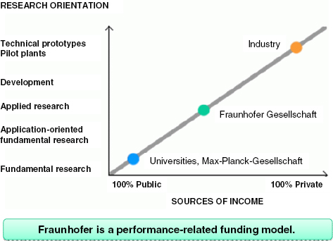
FIGURE 12 Fraunhofer’s place in the R&D ecosystem.
SOURCE: Nolan Browne, Presentation at July 29, 2009, National Academies Symposium
on “State and Regional Innovation Initiatives—Partnering for Photovoltaics Manufacturing
in the United States.â€
but excluded from all but the most basic PV R&D. If we want to help leverage the talent base and investment made in higher education, we have to bridge that gap. We feel that unleashing it will yield major progress.â€
The first reason universities are excluded, he said, is confidentiality. “This is hard to maintain at the university,†he said. “Universities are more open, and it is hard to assign responsibility for disclosures. Generally, this makes a company uncomfortable. There are also national security concerns, like ITAR.â€10
The second problem, he said, is resource mismatch. Aside from the equipment issue, university-sponsored research tends to be “a little inflexible.†That is, it may be difficult for an industry partner to work within the normal academic schedule of a graduate student. “You have to carve out some work that is thesis-sized, or about five years long,†said Mr. Browne. “It can start only when the graduate student gets there, and it ends when he graduates. This puts some friction into the system.â€
____________________
10The International Traffic in Arms Regulations can affect university research activities because it prohibits noncitizens from having access to ITAR-protected technologies or data.
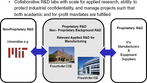
FIGURE 13 Designing the university-industry interface.
SOURCE: Nolan Browne, Presentation at July 29, 2009, National Academies Symposium
on “State and Regional Innovation Initiatives—Partnering for Photovoltaics Manufacturing
in the United States.â€
Problem three is “mission mismatch.†The issue of publication is central, he said. “There’s an extreme difference. MIT or any university would prefer to publish. An industry would very often prefer not to.â€
Dr. Browne said that the Fraunhofer system removed much of the inter-institutional friction. “We want to bridge the valley of death by linking research to both sides of the valley,†he said, “and can accommodate both their needs.†In Germany, there are three sectors: industry, a private, for-profit entity; the universities; and the Max Planck institutes, which are primarily public.11 Fraunhofer gets 30 percent of its income from public sources. It is designed to be “an aggressive applied research lab,†he said. “We have to go out to industry and ask them, what do you need? If industry is not interested in paying that other 70 percent, we have to cut staff. So it forces us to be clear about our mission.â€
In Fraunhofer USA, he said, a university aligns with a Fraunhofer center. In the case of MIT, the scientific director has a faculty position at MIT. There is a professional team, internal to Fraunhofer, which allows in-house research that is not part of the university, including the confidential or ITAR research. A large body of work comes from students who do their thesis work for the university in the CSE laboratory. To accommodate this, the center has three sets of labs:
____________________
11The Max Planck Society for the Advancement of Science, founded in 1948, is an independent nonprofit association of nearly 80 German research institutes. About 84 percent of its funding comes from the federal and state governments.
confidential labs, shared labs, and open labs. This division, he said, is based on the German model.
The Challenges of the German Model
There are challenges, he acknowledged, in bringing the German model to the United States. “My job over the last year has been to adapt it,†Dr. Browne said. First, they forged an MIT-Fraunhofer framework agreement between the two presidents. This addressed the problems listed above as follows:
• Confidentiality concerns: “Fraunhofer controls the terms of how the labs are run,†he said. “Some research is more open and can be published; other research is confidential and won’t be published. The client agrees to all this. This helps us determine how to segment a project into nonconfidential and confidential components. Often what you need to keep secret is just 25 percent, the ‘secret sauce’. The trick is to break up a project and manage it so you can leverage university resources while keeping certain parts confidential.â€
• The resource mismatch: “We basically identify how to share the R&D resources across both institutions. We have a joint R&D template that we use when we go out as to win contracts from industry, and our work with industry is a joint venture.â€
• The mission mismatch: “We as a partnership can provide the flexibility necessary. We preserve the educational mandate of the university while giving industry what it needs.â€
Different Tuition Structures
Several key challenges remained, Dr. Browne said. One is the difference in tuition structures. In Germany, students can work in a Fraunhofer lab without cost to the lab. “In the United States, universities see a student as a profit center. They’re paying $50,000 a year to have that graduate student and they need a return.†The center addresses this through a Fraunhofer-MIT seed grant program. Students are funded jointly to work in the Fraunhofer lab and earn their Ph.D.s there.
Second, universities must learn to accept relationships with intermediary institutions. In Germany, this is not a consideration, because Fraunhofer has existed for 60 years and works with all major firms. For the United States, the new model will require “some success stories†to establish its reputation.
Third, the Fraunhofer model was set up to work with medium and large companies, largely because there are few start-ups in Germany. The United States, by contrast, counts on start-ups for much of its innovation, especially in the Cambridge area. The center will have to develop the custom of interfacing with start-ups.
Dr. Browne said that policy makers could help support this model by providing industrial scholarships to pursue this kind of academic research. “There is currently a bias in universities against applied research,†he said. “The intermediary model could change the whole paradigm.
He also said that just discussing the model could encourage more universities to engage with intermediaries. If applied research capabilities were recognized as desirable for winning government grants or publishing papers, for example, professors would have more incentive to work with such laboratories.
He summarized by saying that the direct interfaces between university and industry can be challenging, but that it is critical to do and “will be very rewarding.†By addressing the confidentiality and research mismatches, he said, “the intermediary institutions can unlock the university resources and support industry.†U.S. policy makers could help develop this model further by addressing the tuition problem and encouraging universities to pursue the partnerships. “In the future,†he said, “to grow these things out, there has to be a sizeable investment from the U.S., because this is the market it’s going to serve in the long run.â€
THE SEMATECH MODEL: POTENTIAL APPLICATIONS FOR PV
Michael Polcari
SEMATECH
Dr. Polcari began with an overview of SEMATECH, of which he is president and CEO. It is a member-driven organization of semiconductor companies, he said, that share the goals of technological innovation and manufacturing productivity. It approaches these objectives by addressing questions throughout the supply chain.
He said that the decreasing cost per function was another way of looking at Moore’s Law. It combines the technology challenges of increasing the number of transistors per area with the productivity challenges of decreasing the cost per area. In the past, he said, driving technology innovation had come mostly from shrinking lithography dimensions, but the emphasis at present is shifting to new materials and device structures.
The Goal of Accelerating Commercialization
A key objective of SEMATECH, Dr. Polcari said, is to accelerate the commercialization of technology. This does not necessarily mean the invention of new devices or structures, but putting in place the infrastructure that allows the semiconductor industry to practice those things: accelerating tool development and materials development, understanding whether all the elements of a technology are ready, and making sure the ones that are lagging are being driven. “In the end,†he said, “that is what accelerates the commercialization.â€
Reducing the cost per function is actually done by attacking productivity challenges, he said. For semiconductors, this can be done in two ways: to increase the area size, which happens about every 12 or 13 years, and to reduce the cost per wafer. “There are a lot of analogies for PV in what we do to drive down costs in semiconductors.â€
The SEMATECH Story
Dr. Polcari turned to the background of SEMATECH. In 1987, he said, essentially two proposals came out of government and industry (from the Defense Science Board and the Semiconductor Industry Association) that coalesced in driving an organization with the features of SEMATECH. These proposals came out of the sharp loss of market share to Japanese companies. By working together, the two sectors were able to set up SEMATECH as a national, not-for-profit consortium to address the problem.
At the beginning, all participants understood there was a problem, but there was no consensus on what it was. About a year was spent in discussing what the group should try to fix, beyond trying to regain market share.
SEMATECH was finally established as a joint industry-government partnership, with each contributing $100 million to the effort. In hindsight, some of the factors that led to success were
• Commitment from top-level executives, both in government and industry, to take this step. Without that commitment, he said, nothing would have happened.
• Industry leadership: This was vital because only industry could identify the problems they needed to solve.
• A clear precompetitive mission: The group needed to work together on the U.S. technology infrastructure.
• Achieving a broad representation of partnerships from industry and government, involvement of the national labs, including NIST, and leveraging of government funds.
A central factor leading to success, he said, was that SEMATECH was member driven. Members decided what the problems were, set the research agenda, and apportioned resources. “It is essential that the people whose problems you’re trying to solve are the ones who decide what you work on,†he said.
Some Successes of SEMATECH
Dr. Polcari listed some of the successes of the strategy. SEMATECH helped the industry to achieve parity and regain the market share from Japan during the late 1980s and early 1990s. Since then, he said, the U.S. industry has been healthy.
An important mechanism behind success, he added, was the semiconductor roadmap, a guide to plans and actions. The roadmap coordinated the industry through several multibillion-dollar transitions:
• Developing next-generation patterning, using advanced technology development, equipment, and materials (193nm dry immersion and EUV).
• The transition to the next wafer size, providing materials readiness and equipment performance metrics.
• Screening and characterization of new materials, including more than 350 material systems for high-k metal gates and more than 500 low-k materials.
“This has allowed members to share not only cost but risk,†he said. “They can see all the results and decide which are the few they want to pursue.â€
He described several other benefits of the program. One was to help member firms by finding the “dry holes. Understanding those things that aren’t going to work can be as important as success,†he said. Also, the organization itself attracted other businesses, creating jobs first around its headquarters in Austin, Texas, and today around Albany, New York, near the new College of Nanoscale Science and Engineering. This attraction has even led to the name “SEMATECH effect†for the process of high-tech job creation. Finally, members have seen significant return on the investment in the consortium. The average member’s ROI has been calculated as about a 5.4 to 1 for what they invest in the form of dues and other payments.
Increasing the Size of the “Ecosystemâ€
Dr. Polcari noted that the reach and size of the SEMATECH “ecosystem†has grown appreciably. “With a large and diverse number [of semiconductor manufacturers] you can set an agenda driven by a consensus. People know this will result in something the industry will utilize.†In addition to increasing the number of semiconductor manufacturers, the consortium has added equipment and materials suppliers, who help set and drive an agenda that interests them, broadening the reach of the group and helping it to be more productive. One advantage of this breadth, he said, is that it convenes a large network around individual problems and brings solutions more quickly. It also facilitates partnerships with universities and government labs, especially NIST and Lawrence Berkeley National Laboratory.
The heart of the program, however, is manufacturing productivity, which is addressed on both strategic and tactical levels. Strategically, companies need to know the most productive architecture for a factory of the future. Tactically, they need to continuously reduce costs in today’s fabs and manage ever-increasing capital, manufacturing, and R&D costs. There are also sustainability challenges,
such as how to reduce the industry’s environmental footprint, find safer materials, and conserve consumables. “All of these challenges,†he said, “ are also relevant to photovoltaic technologies.â€
The Importance of Benchmarking
The way SEMATECH works on those challenges, Dr. Polcari said, is by doing “a lot of benchmarking, where members request data and than have to share it in nondisclosed ways.†They also have a Manufacturing Methods Council that develops and shares best practices, aided by equipment productivity teams, where members identify common problems on a tool or tool set and work together with a supplier. “This turns out to be more efficient than working independently. We also run workshops and ‘councils’ to address common problems, such as finding second sources of spare parts.â€
He discussed benchmarking in more detail because of its importance to members. SEMATECH has developed a system of “blind benchmarking†in which companies have developed 50 metrics they share with each other on a nondisclosed basis. Each knows which data refer to their own company, but not which data refer to other companies. Once the data they want are collected, members have to share data to get data back. Some of them ask for benchmarking on mundane things, such as the cost of electricity. One member, after seeing the utility bills of other companies, approached their power company, demonstrated that their rates were not competitive with those of other companies, and won a reduction. The benchmarking is useful for everybody, even without specific attribution, because every company wants to improve productivity every year. “When you can see that your 10 percent improvement still leaves you behind by 50 or 60 percent,†he said, “you realize you have to do something different.â€
He also cited one company’s experience in saving money through energy conservation. In looking at the performance of a particular tool, they found that most of its power was consumed by the pumps. When they realized how much energy they could save with the pumps in idle mode, they identified which pumps could be idled at various times. They were then able to work with equipment suppliers to adjust the idle modes for maximum efficiency. This information was made available to all members.
Dr. Polcari concluded by saying that a review of the history and present activities of SEMATECH was likely to yield numerous practical lessons for the photovoltaic industry. He said that the SEMATECH model had application not only in technology development but also manufacturing productivity and collaborative strategies that could benefit all participants at the precompetitive level. “Certainly our experience in organizing and recruiting consortia has helped to bring a lot of cost reduction to the industry.â€
THE SEMICONDUCTOR RESEARCH CORPORATION (SRC):
A PROVEN MEANS TO FUND RELEVANT RESEARCH
Larry Sumney
Semiconductor Research Corporation
Mr. Sumney began with a review of Semiconductor Research Corporation (SRC), which was founded in 1982. The immediate impetus for forming SRC was a 1981 Hewlett-Packard study of the reliability and yield of integrated circuits being manufactured at that time. This study concluded that integrated circuits (ICs) produced in the U.S. were inferior in reliability and yield to those from many other countries. A number of reasons were cited: Industry did not have sufficient research capacity; the federal government was reducing funding for and, therefore, universities were not interested in silicon-based IC research. “It was a challenge to generate a pool of faculty with experience in manufacturing and design,†said Mr. Sumney, “or to find educated students familiar with silicon ICs.â€
The research needs seemed to be greater than any single company could address alone. In order to reduce cost and risk of the needed research, industry decided to organize, and pool their resources. This was not an easy step, because the industry was—and is—extremely competitive. Still, they decided they could collaborate on precompetitive, generic research that would help all of them without jeopardizing their competitive positions. They decided to form and join the Semiconductor Research Corporation.
Partnering with Government and Academia
By around 1986, it became clear that SRC would be more productive if all three societal sectors were included—industry, academia, and government. “Looking to the government to leverage the investment of industry has been a major key to ongoing success,†Mr. Sumney said. “And the culture in universities has totally changed since SRC started. We now have university centers that collaborate with other universities. The outcome of this collaboration is excellent, relevant research results.â€
One measure of success has been the publication rate. For example, Mr. Sumney said, in 1981, universities produced only 180 publications on silicon topics, and industry produced 304. In 2008, universities supported by SRC produced 2,226 publications on silicon research. “This has had a tremendous impact over time,†he said. “Each paper has one or more graduate students associated with it, many of whom are hired later by one of our members. So the valley of death is bridged by recruiting students into jobs in industry where they continue to work on research often related to their dissertation.â€
Between the Blue Sky and the Market
Mr. Sumney noted that both industry and universities now have long experience with the basic format of SRC. The research activities of SRC are focused between “blue-sky†basic research and early product development. In general, industry is more tightly focused on nearer-term research, while universities have more autonomy and time to pursue longer-term research. The collaborations are all governed by research contracts, with milestones jointly worked out with the principal investigator. “Negative progress is fine,†he said; “we just need to know about it. In such cases, the partnership has a choice of either changing direction or allowing the work to continue a little longer. The strategy works out well.â€
Over the years, SRC has invested over $1.3 billion contributed by members and government; it has supported more than 7,500 graduate students through 3,000 research contracts, 1,700 faculty, and 241 universities. This support has resulted in more than 43,000 technical documents, 326 patents, 579 software tools, and work on 2,315 research tasks or projects. “The task level is where results come from,†he said. “These may be integrated into a center, or they may be a single professor and several grad students.â€
SRC was recently a recipient of the National Medal of Technology “for building the world’s largest and most successful university research force to support the rapid growth and 10,000-fold advances of the semiconductor industry.†It was also praised “for providing the concept of collaborative research as the first high-tech research consortium, and for creating the concept and methodology that evolved into the International Technology Roadmap for Semiconductors.â€
Agreeing to Collaborate: A Key to Success
Mr. Sumney reviewed the reasons for SRC’s success. The first, and most important, was that competitors agreed to collaborate. “That’s key,†he said, “and it didn’t happen quickly. In our early meetings, you couldn’t get anybody to say anything, because they were afraid of giving out secrets. They had to learn to trust. The CEOs first made the decision to do it, but it took a while to trickle down to the technical people. Today this is one of our strongest features—the collaboration that occurs at technology meetings among our members and involving universities. Our strategic ideas now come from our members, and we are a member-driven organization.â€
Another reason for success was that the research was precompetitive and the IP was shared. The universities own the IP, but they provide SRC members with royalty-free, nonexclusive access. “We make sure there’s no blocking IP,†he said. “We look at everything in the beginning. It took universities a while to get used to this, but a blue-ribbon panel came up with language on IP in 1997 and 1998, working with the presidents and deans of universities. Since then we’ve had little
difficulty.†When selecting research topics, SRC first solicits white papers from the academic research community. If they get 100 to 150 responses, they choose the best 10 or so, solicit full proposals, and work with industry to select the best one or two.
Representing the Whole Value Chain
Because of the way the industry has evolved, SRC represents all parts of the value chain. At the outset, all the members were integrated device manufacturers. Next to join were equipment manufacturers and software providers. Industry began to restructure as fabs became more expensive. Several integrated device manufacturers began to change to “fab-lite†or fabless. Foundries evolved. We now have involvement with all sectors of this evolving industry.
SRC is also accountable to its members, he said. It is evaluated every year by industry members, and periodically by universities. Among universities it is often the “funder of choice,†he said, “having risen from second or third to first for many of them. Member companies consistently rate the organization at about 4.5 on a 1-5 scale of value.â€
Relevance for the Photovoltaic Technologies Industry
Mr. Sumney suggested that the way the semiconductor industry has followed roadmaps and Moore’s Law may have great relevance for the photovoltaic industry. SRC began by securing industry agreement on major needs in all areas: devices, processing, interconnect, packaging, and design. “What Moore’s Law has done,†he said, “is to give the research process a cadence. You try to get from one node, or minimum feature size, to the next as fast as possible. That has served to excite the industry to beat the roadmap, and they have done that. It wouldn’t have happened without that expectation or cadence that Moore’s Law provides. We feel that for PV, this kind of expectation could also be used, along with a roadmap developed with DoE and others.â€
He said that SRC had evolved as a family of distinct but related programs:
• The Global Research Collaboration ensures the vitality of the current industry, supporting shorter-term research (a 7- to 14-year time frame) with traditional CMOS technology.12
____________________
12The complementary metal-oxide-semiconductor (CMOS) transistor is used to manufacture most of the world’s computer chips. While CMOS chips have become steadily smaller, the International Technology Roadmap for Semiconductors (ITRS) predicts that the size limit for CMOS technology is likely to be 5 nm to 10 nm, which may reached in 10 to 15 years. Researchers cannot yet predict which new materials or techniques will allow the rising performance and shrinking size of computer chips to continue.
• The Focus Center Research Program, with a 14- to 20-year time frame, is focused on breaking down barriers to extend CMOS as far as it can go.
• The Nanoelectronics Research Initiative seeks to identify the next information element beyond CMOS.
• The SRC Education Alliance (SRCEA) is a private foundation that provides fellowships and scholarships and supports various programs in physical science and engineering education.
• The Topical Research Collaborations (TRC) is a new SRC research vehicle to apply the collaborative model to new technical areas. One is “The Energy Research Corporation†or TERC, which has a program in photovoltaic research. This will begin with an effort at Purdue University to model and simulate different PV structures to assess their viability. Members currently include Applied Materials and First Solar. A second TRC, “National Institute for Nano-engineering (NINE),†is a joint program with Sandia National Laboratories and interested member companies such as Intel, Exxon Mobil, and Goodyear.
Applying the Collaboration Model
Mr. Sumney suggested that the collaboration model developed for ICs could easily be applied to new technical areas, such as PV. “One reason we’re working on such things is that they bring SRC new members we normally wouldn’t
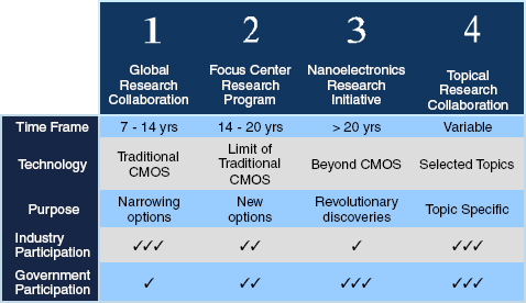
FIGURE 14 Our four major research programs.
SOURCE: Larry Sumney, Presentation at July 29, 2009, National Academies Symposium
on “State and Regional Innovation Initiatives—Partnering for Photovoltaics Manufacturing
in the United States.â€
have. For example, Exxon Mobil would not normally join SRC’s semiconductor program as it exists, but it is interested in PV technologies. Goodyear is another example. Existing members such as IBM and Intel are also interested in TRCs. We’re hoping that this leads to new innovation, new methodologies for collaboration, and valuable results from the universities.â€
PV and semiconductor manufacturing share many features, he said, including
• Common materials, such as silicon ingots and wafers.
• Common equipment, such as tools for etching, sputtering, chemical vapor deposition, metrology tools, defect inspection, testing and assembly.
• Common processes, such as wafer handling and deposition of material and coatings on substrates.
He also described potential technology overlaps, such as thin films, flexible substrates, and novel semiconductor materials. And both sectors of manufacturing research focus on increasing efficiencies and reducing costs.
A Consortium, with Industry Taking the Lead
A possible collaborative model for PV manufacturing research would have many of the same features as SRC. It would bring together industry, universities, and government, including the DoE and NIST labs. These would be well positioned to develop roadmap and technology assessments that identify gaps and common challenges; focus on precompetitive research and the underlying technology needs; and make the research results broadly available to all participants.
This would be done through several approaches. One is to develop an “evolved, high-quality Web site†that would make research results available to the industry membership before publication. Another is to build relationships between the member companies and students, including a mentoring program, opportunities for students to deliver papers at technical meetings, and potential hiring sessions with companies. Coordinating research can minimize overlap, leverage government and university work, and increase the efficiency of the dollars spent.
“In summary,†he said, “we see collaborative research as being much more efficient than people working on their own.†A consortium, can bring the sectors together with government in a PV manufacturing research “ecosystem.†Industries take the lead by jointly identifying the most urgent R&D needs at the precompetitive level, and government can inject incentives through co-funding research. “Given the diversity of participants, this ecosystem can be distributed but very coordinated. We see a flow of related ideas and technologies moving in both directions between industry and academia, with government playing a major role.â€
PV TECHNOLOGY ROADMAPS AND INDUSTRY STANDARDS: AN ASSOCIATION’S APPROACH
Bettina Weiss
PV Group
Ms. Weiss began by defining the PV Group, which had newly emerged from the larger group SEMI, which, in turn, was founded nearly 40 years ago as a global semiconductor industry association. Most of approximately 2,000 member companies represent the semiconductor-manufacturing sector. Over the years, the group has expanded into the fields of flat-panel display and micro-electromechanical systems, and related technologies. During the past two years, it has moved into photovoltaic technologies as well and established PV Group as its global photovoltaic initiative. “PV Group captures the 30 percent or so of SEMI’s members that are active in PV,†she said, “and provides services and products in the area of public policy, market research, standardization, industry collaboration, education and eventsâ€
Unique Challenges of PV
PV presents unique challenges, Ms. Weiss said. The field is “very policy driven,†especially in the United States. The industry structure is still not well defined, with a mix of very small to very large companies operating in different technologies and markets and focusing on different manufacturing targets. The industry suffers from deployment bottlenecks and very high logistics costs, especially for transport of modules and panels. “It will be a while before all this shakes out,†she said, “and as an association maybe we can lend a calming voice to the fray. We feel we can best address these issues if the industry stakeholders work together.â€
She said that the PV industry is likely to “ benefit tremendously from the chip experience.†The PV segment within SEMI has grown significantly, largely because semiconductor and flat panel display equipment and materials suppliers have moved into the PV space, and cell and module manufacturers have joined the discussion and begun to actively contribute and weigh in. “We’re supporting those members, and we also see an influx of pure players in the PV industry. The combination of those two has generated a lot of ideas about what has to be done in standards, public policy, and other areas. The end goals for all participants,†she said, “are the same: to accelerate commercialization, reduce manufacturing costs, and shorten the path to mass deployment of solar energy to the greater population.â€
Current Opportunities for the Industry
Ms. Weiss said she would focus her comments on how the PV Group could help expand core competencies in the PV industry. She said that opportunities exist in several key areas:
• Industry standards that reduce cost and spur innovation.
• Industry information that guides investment and planning decisions.
• Industry advocacy and promotion.
• Buyer-seller collaboration on critical issues.
• Developing a greener and more robust supply chain.
“Overall,†she said, “it is about effective buyer and seller collaboration, and finding commonalities where we can do more together faster and better.â€
The PV Group strategy is guided by SEMI’s international board of directors and, more directly, by PV Advisory Committees representing equipment and materials suppliers, cell and module manufacturers, and other interests. Because the PV industry is global, an objective is to align U.S. interests, based on global trade conditions and developments. “To build the U.S. industry,†she said, “collaboration among U.S. firms is critical, as are global partnerships. We need these to strengthen the U.S. supply chain and bring the ‘green-collar jobs’ we desperately need.†The position of PV Group, she said, is that collaboration between industry and government will improve global partnerships as well as national ones. But available funding now should be directed toward strengthening U.S. manufacturing platforms and their member-driven organizations, including SRC, SEMI, PV Group, and others.
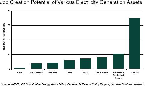
FIGURE 15 U.S. solar job potential.
SOURCE: Bettina Weiss, Presentation at July 29, 2009, National Academies Symposium
on “State and Regional Innovation Initiatives—Partnering for Photovoltaics Manufacturing
in the United States.â€
Early Discussions of a Roadmap
Referring to a joint PV Group-DoE workshop held in San Francisco in July 2009, Ms. Weiss noted “an appetite, a readiness†in the United States to develop a domestic or even international roadmap, perhaps modeled on ITRS of the semiconductor industry. The workshop broke into groups represented different sectors of the supply chain, and each was asked to consider three questions:
• What are the key barriers to success in the U.S. PV industry?
• Which ones would benefit from a collaboration approach?
• Would a roadmap be the right tool to do that?
She said that the answer to #3 was a resounding yes, with a unanimous show of hands. She also noted that this should have further validation from the cell and module communities, which were underrepresented. Attendees and others were now considering how to structure, fund, and govern this process.
An Urge to Kick-Start Standards
The first topic that PV Group’s members wanted to kick-start was standards, she said. “We know from the ITRS experience that many hundreds of standards and safety guidelines have been generated because of the semiconductor roadmap and the information it provided.†These standards helped improve interfaces, tool-to-tool communication, process and materials efficiencies, operating risks, environmental contamination, and other parameters.
She gave a short history of SEMI, which was established in 1970. Its standards program was established three years later, primarily to address the issue of wafer specification. There were then about 2,000 wafer specs in use, she said, and the industry saw that this was causing too much waste at a time of silicon shortage. “This propelled us into the standards business,†she said, beginning with an agreement to use a single size of wafer. Standard setting has evolved over the years as members have moved into other areas, such as flat panel display, MEMS, and now PV.
For PV, standards were the first initiative that SEMI members wanted to work on. She said that about 400 people were working on this globally, beginning with a PV Standards Committees formed in Europe in 2007, followed by a group in North America later that year and Taiwan and Japan in 2009. SEMI has published almost 800 documents on test methods, specifications, equipment and materials safety, and other topics. The PV Group had concluded that about 64 out of SEMI’s 80 major categories were applicable to crystalline silicon-based PV, including hundreds of specifications and test methods, so that existing semiconductor standards can be applied directly to PV. “The PV industry can derive immediate benefits from using existing standards now,†she said.
Moving Up a Steep Learning Curve
Among priorities and gaps, Ms. Weiss said, were automation, environmental health and safety (EHS), and the conversion of older facilities, such as 200 mm fabs. All could benefit from dissemination of standards and best practices. She emphasized the need for further discussion of the EHS challenge. “I think we’re dealing with a lot of really nasty substances in the manufacturing line,†she said. “We need to talk more about how to reduce volume, make them safer, develop better emergency response systems, the end-of-life cycle, recycling, and helping business take back its tools so that nothing ends up in the ground or in the air.â€
She concluded with the “message that the learning curve we are all on is a very steep one, but it can be accelerated by collaboration. We invite all of your organizations to talk to us at PV Group. We’re willing to help, and we have national as well as international arms we can utilize.â€
DISCUSSION
Comparing Semiconductors and Photovoltaic Technologies
Dan Josell of NIST drew a contrast between the role of SEMATECH and the condition of the PV industry. With SEMATECH, he said, “We were starting with a technology that was top of the line, with high profit margins. Here you’re starting with something that’s basically a commodity. Energy is already provided by half a dozen dominant technologies, none of which is solar. So are there differences in trying to get together industries that are trying to compete on margins where there will soon be many others on these same price lines.â€
Dr. Polcari replied that there are memory suppliers who collaborate today, including Toshiba and Samsung, both of which work with IBM. “The question is, can you collaborate on things early on that can save dollars on manufacturing,†he said. “If there are areas they all need to work on, there’s no point in everyone working separately unless there is a competitive edge. There always seem to be areas like that, such as vacuum systems and air handling. These may not be the best examples, but the right ones will likely come out of roadmapping.â€
Mr. Sumney said he agreed, using the example of Micron, a commodity memory manufacturer that has been involved in SRC’s Focus Center Research Program for 12 years. “We’re holding a memory workshop in October,†he said, “and they were one of the first companies to sign up. So I see that the commodity manufacturers are getting enough out of this to be very interested.â€
PV as a Commodity Industry
Dr. Empedocles noted that PV has lower equipment requirements than the semiconductor industry, which indicates both that “it’s more of a commodity
industry†and is also an industry that requires a much smaller investment. He said that SVTC Solar had met with more than 100 PV companies, and their largest concern was the investment community’s reluctance to act during the early months when there are still uncertainties about “whether the technology will be manufacturable.†Even though the funds required might not be large compared with the semiconductor industry, they are large for individual PV companies. “This is a real barrier that a shared facility can help with.†He noted that standardization would be difficult while the industry is divided into the two categories of thin-film and wafer technologies, but that the industry would probably need to standardize more as it matures.
Mr. Engardio recalled the earlier accounts of how fast the industry as a whole is moving down the cost curve. “I guess the question is, could this be accelerated through collaboration.â€
Dr. Wessner said it was important to note that both joining and contributing to earlier consortia had been voluntary. “If there’s willingness to join, there is clearly a perception of common good,†he said. “But I think we have to be careful talking about commodity industries. Oil is described as a commodity, but as Mexico and Iraq demonstrate, it’s difficult to maintain production without the latest technologies.†He noted that Micron is a commodity company whose production excellence enables it to compete globally—and yet they choose to participate in the SRC. He said it would be interesting to know how well such a company would do without access to these institutions.


