
NOTE: Reprinted from Robert H. Dennard, Fritz H. Gaensslen, Hwa-Nien Yu, V. Leo Rideout, Ernest Bassous, and Andre R. LeBlanc, 1974, Design of ion-implanted MOSFETS with very small physical dimensions, IEEE Journal of Solid State Circuits 9(5):256 with permission of IEEE and Robert H. Dennard © 1974 IEEE.
Design of Ion-Implanted MOSFET’s with Very Small Physical Dimensions
ROBERT H. DENNARD, MEMBER. IEEE, FRITZ H. GAENSSLEN, HWA-NIEN YU, MEMBER, IEEE, V. LEO RIDEOUT, MEMBER, IEEE, ERNEST BAS SOUS, AND ANDRE R, LEBLANC, MEMBER, IEEE
Classic Paper
This paper considers the design, fabrication, and characterization of very small MOSFET switching devices suitable for digital integrated circuits using dimensions of the order of 1 μ. Scaling relationships are presented which show how a conventional MOSFET can be reduced in size. An improved small device structure is presented that uses ion implantation to provide shallow source and drain regions and a nonuniform substrate doping profile. One-dimensional models are used to predict the substrate doping profile and the corresponding threshold voltage versus source voltage characteristic. A two-dimensional current transport model is used to predict the relative degree of short-channel effects for different device parameter combinations. Polysilicon-gate MOSFET’s with channel lengths as short as 0.5 μ were fabricated, and the device characteristics measured and compared with predicted values. The performance improvement expected from using these very small devices in highly miniaturized integrated circuits is projected.
I. LIST OF SYMBOLS
|
α |
Inverse semilogarithmic slope of subthreshold characteristic. |
|
D |
Width of idealized step function profile for channel implant. |
|
ΔWf |
Work function difference between gate and substrate. |
|
∈Si, ∈OX |
Dielectric constants for silicon and silicon dioxide. |
|
Id |
Drain current. |
|
k |
Boltzmann’s constant |
|
κ |
Unitless scaling constant. |
|
L |
MOSFET channel length. |
|
µeff |
Effective surface mobility. |
|
ni |
Intrinsic carrier concentration. |
|
Na |
Substrate acceptor concentration. |
|
Ψs |
Band bending in silicon at the onset of strong inversion for zero substrate voltage. |
|
Ψb |
Built-in junction potential. |
|
q |
Charge on the electron. |
|
Qctt |
Effective oxide charge. |
|
tox |
Gate oxide thickness. |
|
T |
Absolute temperature. |
|
Vd, Vs, Vg, Vsub |
Drain, source, gate and substrate voltages. |
|
Vds |
Drain voltage relative to source. |
|
Vs—sub |
Source voltage relative to sustrate. |
|
Vt |
Gate threshold voltage. |
|
Ws, Wd |
Source and drain depletion layer widths. |
|
W |
MOSFET channel width. |
This paper is reprinted from IEEE JOURNAL OF SOLID-STATE CIRCUITS, vol. SC-9, no. 5, pp. 256–268, October 1974.
Publisher Item Identifier S 0018-9219(99)02196-9.
II. INTRODUCTION
New high resolution lithographic techniques for forming semiconductor integrated circuit patterns offer a decrease in linewidth of five to ten times over the optical contact masking approach which is commonly used in the semiconductor industry today. Of the new techniques, electron beam pattern writing has been widely used for experimental device fabrication [1]-[4] while X-ray lithography [5] and optical projection printing [6] have also exhibited high-resolution capability. Full realization of the benefits of these new high-resolution lithographic techniques requires the development of new device designs, technologies, and structures which can be optimized for very small dimensions.
This paper concerns the design, fabrication, and characterization of very small MOSFET switching devices suitable for digital integrated circuits using dimensions of the order of 1 μ. It is known that reducing the source-to-drain spacing (i.e., the channel length) of an FET leads to undesirable changes in the device characteristics. These changes become significant when the depletion regions surrounding the source and drain extend over a large portion of the region in the silicon substrate under the gate electrode. For switching applications, the most undesirable “short-channel” effect is a reduction in the gate threshold voltage at which the device turns on, which is aggravated
by high drain voltages. It has been shown that these short-channel effects can be avoided by scaling down the vertical dimensions (e.g., gate insulator thickness, junction depth, etc.) along with the horizontal dimensions, while also proportionately decreasing the applied voltages and increasing the substrate doping concentration [7], [8]. Applying this scaling approach to a properly designed conventional-size MOSFET shows that a 200-Å gate insulator is required if the channel length is to be reduced to 1 µ.
A major consideration of this paper is to show how the use of ion implantation leads to an improved design for very small scaled-down MOSFET’s. First, the ability of ion implantation to accurately introduce a low concentration of doping atoms allows the substrate doping profile in the channel region under the gate to be increased in a controlled manner. When combined with a relatively lightly doped starting substrate, this channel implant reduces the sensitivity of the threshold voltage to changes in the source-to-substrate (“backgate”) bias. This reduced “substrate sensitivity” can then be traded off for a thicker gate insulator of 350-Å thickness which tends to be easier to fabricate reproducibly and reliably. Second, ion implantation allows the formation of very shallow source and drain regions which are more favorable with respect to start-channel effects, while maintaining an acceptable sheet resistance. The combination of these features in an all-implanted design gives a switching device which can be fabricated with a thicker gate insulator if desired, which has well-controlled threshold characteristics, and which has significantly reduced interelectrode capacitances (e.g., drain-to-gate or drain-to-substrate capacitances).
This paper begins by describing the scaling principles which are applied to a conventional MOSFET to obtain a very small device structure capable of improved performance. Experimental verification of the scaling approach is then presented. Next, the fabrication process for an improved scaled-down device structure using ion implantation is described. Design considerations for this all-implanted structure are based on two analytical tools: a simple one-dimensional model that predicts the substrate sensitivity for long channel-length devices, and a two-dimensional current-transport model that predicts the device turn-on characteristics as a function of channel length. The predicted results from both analyses are compared with experimental data. Using the two-dimensional simulation, the sensitivity of the design to various parameters is shown. Then, detailed attention is given to an alternate design, intended for zero substrate bias, which often some advantages with respect to threshold control. Finally, the paper concludes with a discussion of the performance improvements to be expected from integrated circuits that use these very small FET’s.
III. DEVICE SCALING
The principles of device scaling [7], [8] show in a concise manner the general design trends to be followed in decreasing the size and increasing the performance of MOSFET switching devices. Fig. 1 compares a state-of-the-art n-channel MOSFET [9] with a scaled-down device designed following the device scaling principles to be described later. The larger structure shown in Fig. 1(a) is reasonably typical of commercially available devices fabricated by using conventional diffusion techniques. It uses a 1000-Å gate insulator thickness with a substrate doping and substrate bias chosen to give a gate threshold voltage Vt of approximately 2 V relative to the source potential. A substrate doping of 5×1015 cm–3 is low enough to give an acceptable value of substrate sensitivity. The substrate sensitivity is an important criterion in digital switching circuits employing source followers because the design becomes difficult if the threshold voltage increases by more than a factor of two over the full range of variation of the source voltage. For the device illustrated in Fig. 1(a), the design parameters limit the channel length L to about 5 µ. This restriction arises primarily from the penetration of the depletion region surrounding the drain into the area normally controlled by the gate electrode. For a maximum drain voltage of approximately 12–15 V this penetration will modify the surface potential and significantly lower the threshold voltage.
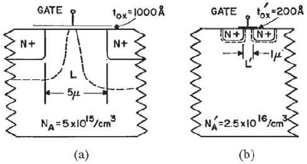
Fig. 1. Illustration of device staling principle with κ = 5. (a) Conventional commercially available device structure, (b) Scaled-down device structure.
In order to design a new device suitable for smaller values of L, the device is scaled by a transformation in three variables: dimension, voltage, and doping. First, all linear dimensions are reduced by a unit less scaling factor κ, e.g., ![]() where the primed parameters refer to the new scaled-down device. This reduction includes vertical dimensions such as gate insulator thickness, junction depth, etc., as well as the horizontal dimensions of channel length and width. Second, the voltages applied to the device are reduced by the same factor (e.g.,
where the primed parameters refer to the new scaled-down device. This reduction includes vertical dimensions such as gate insulator thickness, junction depth, etc., as well as the horizontal dimensions of channel length and width. Second, the voltages applied to the device are reduced by the same factor (e.g., ![]() ). Third, the substrate doping concentration is increased, again using the same scaling factor (i.e.,
). Third, the substrate doping concentration is increased, again using the same scaling factor (i.e., ![]() ). The design shown in Fig. 1(b) was obtained using κ = 5 which corresponds to the desired reduction in channel length to 1 µ.
). The design shown in Fig. 1(b) was obtained using κ = 5 which corresponds to the desired reduction in channel length to 1 µ.
The scaling relationships were developed by observing that the depletion layer widths in the scaled-down device are reduced in proportion to the device dimensions due to the reduced potentials and the increased doping. For example
![]()
The threshold voltage at turn-on [9] is also decreased in direct proportion to the reduced device voltages so that
the device will function properly in a circuit with reduced voltage levels. This is shown by the threshold voltage equation for the scaled-down device
In (2) the reduction in Vt is primarily due to the decreased insulator thickness tox/κ while the changes in the voltage and doping terms lend to cancel out. In most cases of interest (i.e., poly silicon gates of doping type opposite to that of the substrate or aluminum gates on p-type substrates) the work function difference ΔWf is of opposite sign, and approximately cancels out ![]() is the band bending in the silicon (i.e., the surface potential) at the onset of strong inversion for zero substrate bias. It would appear that the
is the band bending in the silicon (i.e., the surface potential) at the onset of strong inversion for zero substrate bias. It would appear that the ![]() terms appearing in (1) and (2) prevent exact scaling since they remain approximately constant, actually increasing slightly due to the increased doping since
terms appearing in (1) and (2) prevent exact scaling since they remain approximately constant, actually increasing slightly due to the increased doping since ![]()
![]() However, the fixed substrate bias supply normally used with n-channel devices can be adjusted so that
However, the fixed substrate bias supply normally used with n-channel devices can be adjusted so that ![]() Thus, by scaling down the applied substrate bias more than the other applied voltages, the potential drop across the source or drain junctions, or across the depletion region under the gate, can be reduced by κ.
Thus, by scaling down the applied substrate bias more than the other applied voltages, the potential drop across the source or drain junctions, or across the depletion region under the gate, can be reduced by κ.
All of the equations that describe the MOSFET device characteristics may be scaled as demonstrated above. For example, the MOSFET current equation [9] given by
is seen to be reduced by a factor of κ, for any given set of applied voltages, assuming no change in mobility. Actually, the mobility is reduced slightly due to increased impurity scattering in the heavier doped substrate.
It is possible to generalize the scaling approach to include electric field patterns and current density. The electric field distribution is maintained in the scaled-down device except for a change in scale for the spatial coordinates. Furthermore, the electric field strength at any corresponding point is unchanged because V/x = V′/x′. Thus, the carrier velocity at any point is also unchanged due to scaling and, hence, any saturation velocity effects will be similar in both devices, neglecting microscopic differences due to the fixed crystal lattice dimensions. From (3). since the device current is reduced by κ, the channel current per unit of channel width W is unchanged by scaling. This is consistent with the same sheet density of carriers (i.e., electrons per unit gate area) moving at the same velocity. In the vicinity of the drain the carriers will move away from the surface to a lesser extent in the new device, due to the shallower diffusions. Thus, the density of mobile carriers per unit volume will be higher in the space-charge region around the drain complementing the higher density of immobile charge due to the heavier doped substrate. Other scaling relationships for power density, delay time, etc., are given in Table 1 and will be discussed in a subsequent section on circuit performance.
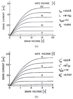
Fig. 2. Experimental drain voltage characteristics for (a) conventional, and (b) scaled-down structures shown in Fig. 1 normalized to W/L = 1.
In order to verify the scaling relationships, two sets of experimental devices were fabricated with gate insulator of 1000 and 200 Á (i.e., κ = 5). The measured drain voltage characteristics of these devices, normalized to W/L = 1 are shown in Fig. 2. The two sets of characteristics are quite similar when plotted with voltage and current scale of the smaller device reduced by a factor of five, which confirms the scaling predictions. In Fig. 2, the exact match on the current scale is thought to be fortuitous since there is some experimental uncertainly in the magnitude of the channel length used to normalize the characteristics (see Appendix). More accurate data from devices with Larger width and length dimensions on the same chip shows an approximate reduction of ten percent in mobility for devices with the heavier doped substrate. That the threshold voltage also scales correctly by a factor of five is verified in Fig. 3, which shows the experimental ![]() versus Vg turn-on characteristics for the original and the scaled-down devices. For the cases shown, the drain voltage is large enough to cause pinchoff and the characteristics exhibit the expected linear relationship. When projected to intercept the gate voltage axis this linear relationship defines a threshold voltage useful for most logic circuit design purposes.
versus Vg turn-on characteristics for the original and the scaled-down devices. For the cases shown, the drain voltage is large enough to cause pinchoff and the characteristics exhibit the expected linear relationship. When projected to intercept the gate voltage axis this linear relationship defines a threshold voltage useful for most logic circuit design purposes.
One area in which the device characteristics fail to scale is in the subthreshold or weak inversion region of the turn-on characteristic. Below threshold. Id is exponentially dependent on Vg with an inverse semilogarithmic slope, α
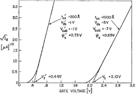
Fig. 3. Experimental turn-on characteristics for conventional and scaled-down devices shown in Fig. 1 normalized to W/L = 1.
[10], [11] which for the scaled-down device is given by
which is the same as for the original larger device. The parameter α is important to dynamic memory circuits because it determines the gate voltage excursion required to go from the low current “off” state to the high current “on” state [11]. In an attempt to also extend the linear scaling relationships to a one could reduce the operating temperature in (4) (i.e., T′ = T/κ), but this would cause a significant increase in the effective surface mobility [12] and thereby invalidate the current scaling relationship of (3), In order to design devices for operation at room temperature and above, one must accept the fact that the subthreshold behavior does not scale as desired. This nonscaling property of the subthreshold characteristic is of particular concern to miniature dynamic memory circuits which require low source-to-drain leakage currents.
IV. ION-IMPLANTED DEVICE DESIGN
The scaling considerations just presented lead to the device structure with a 1-µ channel length shown in Fig. 4(a). In contrast, the corresponding improved design utilizing the capability afforded by ion implantation is shown in Fig. 4(b). The ion-implanted device uses an initial substrate doping that is lower by about a factor of four, and an implanted boron surface layer liming a concentration somewhat greater than the concentration used throughout the unimplanted structure of Fig. 4(a), The concentration and the depth of the implanted surface layer are chosen so that this heavier doped region will be completely within lite surface depletion layer when the device is turned on with the source grounded. Thus, when the source is biased above ground potential, the depletion layer will extend deeper into lite lighter doped substrate, and the additional exposed “bulk” charge will be reasonably small and will cause only a modest increase in the gate-to-source voltage required to turn on the device. With this improvement in substrate sensitivity the gate insulator thickness can be increased to as much as 350 Å and still maintain a reasonable gate threshold voltage as will be shown later.
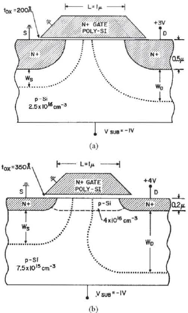
Fig. 4. Detailed cross sections for (a) scaled-down device structure, and (b) corresponding ion-implanted device structure.
Another aspect of the design philosophy is to use shallow implanted n+ regions of depth comparable to the implanted p-type surface layer. The depletion regions under the gate electrode at the edges of the source and drain are then inhibited by the heavier doped surface layer, roughly pictured in Fig. 4(b), for the case of a turned-off device. The depletion regions under the source and drain extend much further into the lighter doped substrate. With deeper junctions these depletion regions would tend to merge in the lighter doped material which would cause a loss of threshold control or, in the extreme, punchthrough at high drain voltages. However, the shallower junctions give a more favorable electric field pattern which avoids these effects when the substrate doping concentration is properly chosen (i.e., when it is not too light).
The device capacitances are reduced with the ion-implanted structure due to the increased depletion layer width separating the source and drain from the substrate [cf. Figs. 4(a) and 4(b)], and due to the natural self-alignment afforded by the ion implantation process which reduces the overlap of the polysilicon gate over the source and drain regions. The thicker gate insulator also gives reduced gate capacitance, but the performance benefit in this respect is
offset by the decreased gate field. To compensate for the thicker gate oxide and the expected threshold increase, a design objective for maximum drain voltage was set at 4 V for tile ion-implanted design in Fig. 4(b), compared to 3 V for the scaled-down device of Fig. 4(a).
V. FABRICATION OF ION-IMPLANTED MOSFET’s
The fabrication process for the ion-implanted MOSFET’s used in this study will now be described. A four-mask process was used to fabricate polysilicon-gate, n-channel MOSFET’s on a test chip which contains devices with channel lengths ranging from 0.5 to 10 µ. Though the eventual aim is to use electron-beam pattern exposure, it was more convenient to use contact masking with high quality master masks for process development. For this purpose high resolution is required only for the gate pattern which uses lines as small as 1.5 µ which are reduced in the subsequent processing. The starting substrate resistivity was 2 Ω · cm (i.e., about 7.5×l015 cm–3). The method of fabrication for the thick oxide isolation between adjacent FET’s is not described as it is not essential to the work presented here, and because several suitable techniques are available. Following dry thermal growth of the gate oxide, low energy (40 keV). low dose (6.7K 1011 atoms/cm2) B11 ions were implanted into the wafers, raising the boron doping near the silicon surface. All implantations were performed after gate oxide growth in order to restrict diffusion of the implanted regions.
After the channel implantation, a 3500-Å thick polysilicon layer was deposited, doped n+, and the gate regions delineated. Next. n+ source and drain regions 2000-Å deep were formed by a high energy (100 keV), high dose (4×l015 atoms/cm2) As75 implantation through the same 350-Å oxide layer. During this step, however, the polysilicon gate masks the channel region from the implant, absorbing all of the As75 dose incident there. The etching process used to delineate the gates results in a sloping sidewall which allows a slight penetration of As75 ions underneath the edges of the gates, The gate-to-drain (or source) overlap is estimated to be of the order of 0.2 µ. The high temperature processing steps that follow the implantations include 20 min at 900°C, and 11 min at 1000°C, which is more than adequate to anneal out the implantation damage without greatly spreading out the implanted doses. Typical sheet resistances were 50 Ω/⟩ for the source and drain regions, and 40 Ω/⟩ for the polysilicon areas. Following the As75 implant, a final insulating oxide layer 2000-Å thick was deposited using low-temperature chemical-vapor deposition. Then, the contact holes to the n+ and polysilicon regions were defined, and the metalization was applied and delineated. Electrical contact directly to the shallow implanted source and drain regions was accomplish by a suitably chosen metallurgy to avoid junction penetration due to alloying during the final annealing step. After metalization an annealing step of 400°C for 20 min in forming gas was performed to decrease the fast-state density.
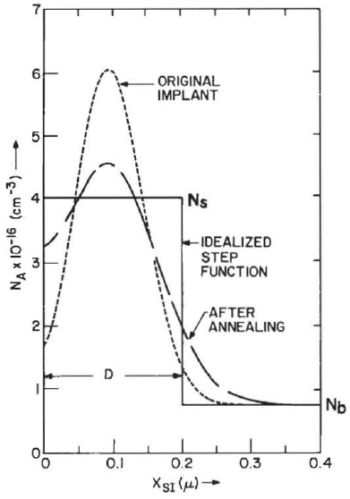
Fig. 5. Predicted substrate doping profile for basic ion-implanted device design for 40 keV B11 ions implanted through the 350-Å gate insulator.
VI. ONE-DIMENSIONAL (LONG CHANNEL) ANALYSIS
The substrate doping profile for the 40 keV, 6.7×10¹¹ atoms/cm2 channel implant incident on the 350-Å gate oxide, is shown in Fig. 5. Since the oxide absorbs 3 percent of the incident dose, the active dose in the silicon is 6.5×10¹¹ atoms/cm2. The concentration at the time of the implantation is given by the lightly dashed Gaussian function added to the background doping level, Nv. For 40 keV B11 ions, the projected range and standard deviation were taken as 1300 Å and 500 Å, respectively [13]. After the heat treatments of the subsequent processing, the boron is redistributed as shown by the heavier dashed line. These predicted profiles were obtained using a computer program developed by F. F. Morehead of our laboratories. The program assumes that boron atoms diffusing in the silicon reflect from the silicon-oxide interface and thereby raise the surface concentration. For modeling purposes it is convenient to use a simple, idealized, step-function representation of the doping profile, as shown by the solid line in Fig. 5. The step profile approximates the final predicted profile rather well and offers the advantage that it can be described by a few simple parameters. The three profiles shown in Fig. 5 all have the same active dose.
Using the step profile, a model for determining threshold voltage has been developed from piecewise solutions of Poisson’s equation with appropriate boundary conditions [11], The one-dimensional model considers only the vertical dimension and cannot account for horizontal short-channel effects, Results of the model are shown in Fig. 6 which plots the threshold voltage versus source-to-substrate bias
for the ion-implanted step profile shown in Fig. 5, For comparison. Fig. 6 also shows the substrate sensitivity characteristics for the nonimplanted device with a 200-Å gate insulator and a constant background doping, and for a hypothetical device having a 350-Å gate insulator like the implanted structure and a constant background doping like the nonimplanted structure. The nonimplanted 200-Å case exhibits a low substrate sensitivity, but the magnitude of the threshold voltage is also low. On the other hand, the nonimplanted 350-Å case shows a higher threshold, but with an undesirably high substrate sensitivity. The ion-implanted case offers both a sufficiently high threshold voltage and a reasonably low substrate sensitivity, particularly for Vs–sub ≥ l V. For Vs–sub < 1 V, a steep slope occurs because the surface inversion layer in the channel is obtained while the depletion region in the silicon under the gate does not exceed D, the step width of the heavier doped implanted region. Vs–sub ≥ l V, at inversion the depletion region now extends into the lighter doped substrate and the threshold voltage then increases relatively slowly with Vs-sub[11]. Thus, with a fixed substrate bias of –1 V, the substrate sensitivity over the operating range of the source voltage (e.g., ground potential to 4 V) is reasonably low and very similar to the slope of tine nonimplanted 200-Å design. However, the threshold voltage is significantly higher for the implanted design which allows adequate design margin so that, under worst case conditions (e.g., short-channel effects which reduce the threshold considerably), the threshold will still be high enough so that the device can be turned off to a negligible conduction level as required for dynamic memory applications.
Experimental results are also given in Fig, 6 from measurements made on relatively long devices (i.e., L = 10 µ) which have no short-channel effects. These data agree reasonably well with the calculated curve. A 35 keV. 6×10¹¹ atoms/cm2 implant was used to achieve this result, rather than the slightly higher design value of 40 keV and 6.7×l011 atoms/cm2.
VII. TWO-DIMENSIONAL (SHOFT CHANNEL) ANALYSIS
For devices with sufficiently short-channel lengths, the one-dimensional model is inadequate to account for the threshold voltage lowering due to penetration of the drain field into the channel region normally controlled by the gate. While some models have been developed which account for tills behavior [14], the problem is complicated for the ion-implanted structure by the nonuniform doping profile which leads to an electric field pattern that is difficult to approximate. For the ion-implanted case, the two-dimensional numerical current transport model of Kennedy and Mock [15], [16] was utilized. The computer program was modified by W. Chang and P. Hwang [17] to handle the abrupt substrate doping profiles considered for these devices.
The numerical current transport model was used to calculate the turn-on behavior of the ion-implanted device by a point-by-point computation of the device current for increasing values of gate voltage. Calculated results are shown in Fig. 7 for two values of channel length in the range of 1 µ, as well as for a relatively long-channel device with L = 10 µ. All eases were normalized to a width-to-length ratio of unity, and a drain voltage of 4 V was used in all cases. As the channel length is reduced to the order of 1 µ, the turn-on characteristic shifts to a lower gate voltage due to a lowering of the threshold voltage, The threshold voltage occurs at about 10–7 A where the turn-on characteristics make a transition front the exponential subthreshold behavior (a linear response on this semilogarithmic plot) to the ![]() square-law behavior. This current level can also be identified from Fig. 3 as the actual current at the projected threslrold voltage, Vt. When the computed characteristics were plotted in the manner of Fig. 3 they gave 4×l0– A at threshold for all device lengths. The band bending, ψs, at this threshold condition is approximately 0.75 V. Some of the other device designs considered with heavier substrate concentrations gave a higher current at threshold, so, for simplicity, the value of 10–7 A was used in all cases with a resultant small error in Vt.
square-law behavior. This current level can also be identified from Fig. 3 as the actual current at the projected threslrold voltage, Vt. When the computed characteristics were plotted in the manner of Fig. 3 they gave 4×l0– A at threshold for all device lengths. The band bending, ψs, at this threshold condition is approximately 0.75 V. Some of the other device designs considered with heavier substrate concentrations gave a higher current at threshold, so, for simplicity, the value of 10–7 A was used in all cases with a resultant small error in Vt.
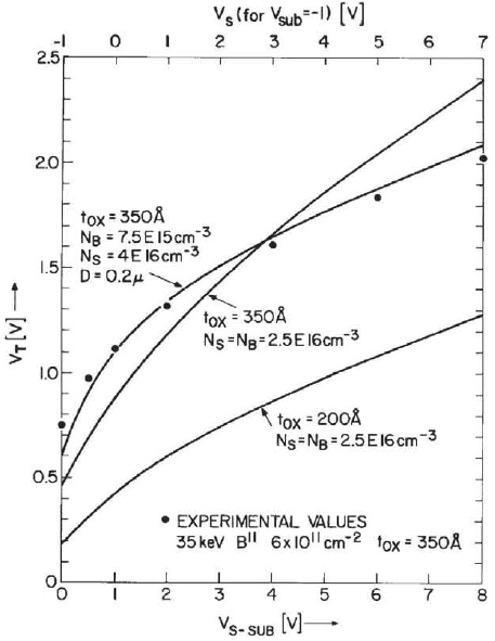
Fig. 6. Calculated and experimental substrate sensitivity characteristics for non-implanted devices with 200- and 350-Å gate insulators, and for corresponding ion-implanted device with 350-Å gate insulator.
MOSFET’s with various channel lengths were measured to test the predictions of the two-dimensional model. The technique for experimentally determining the channel length for very short devices is described in the Appendix.
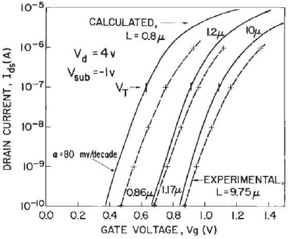
Fig. 7. Calculated and experimental subthreshold turn-on characteristic for basic ion-implanted design for various channel lengths with Vsub = –1 V, Vd = 4 V.
The experimental results are plotted in Fig. 7 and show good agreement with the calculated curves, especially considering the somewhat different values of L. Another form of presentation of this data is shown in Fig. 8 where the threshold voltage is plotted as a function of channel length. The threshold voltage is essentially constant for L > 2 µ, and falls by a reasonably small amount as L is decreased from 2 to 1 µ, and then decreases more rapidly with further reductions in L. For circuit applications the nominal value of L could be set somewhat greater than 1 µ so that, over an expected range of deviation of L, the threshold voltage is reasonably well controlled. For example, L = 1.3 ± 3 µ would give Vt = 1.0 ± 0.1 V from chip to chip due to this short-channel effect alone. This would be tolerable for many circuit applications because of the tracking of different devices on a given chip, if indeed this degree of control of L can be achieved The experimental drain characteristics for an ion-implanted MOSFET with a 1.1-µ channel length are shown in Fig. 9 for the grounded source condition. The general shape of the characteristics is the same as those observed for much larger devices. No extraneous short-channel effects were observed for drain voltages as large as 4 V. The experimental data in Figs. 6-9 were taken from devices using a B11 channel implantation energy and dose of 35 keV and 6.0×10¹¹ atoms/cm2, respectively.
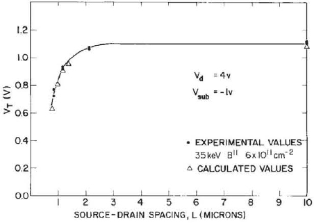
Fig. 8. Experimental and calculated dependence of threshold voltage on channel length for basic ion-implanted design with Vsub = –1 V, Vd = 4 V.
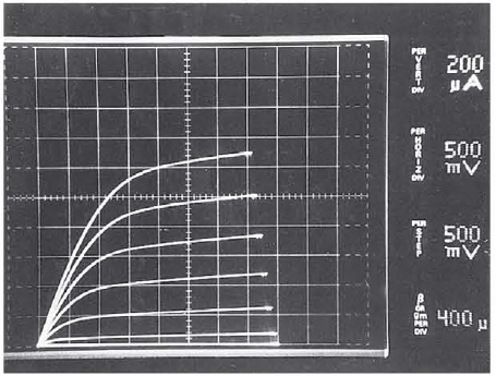
Fig. 9. Experimental drain voltage characteristics for basic ion-implanted design with Vsub = –1 V, L = 1.1 µ, and W = 12.2 µ. Curve tracer parameters; load resistance 30 Ω, drain voltage 4 V, gate voltage 0–4 in 8 steps each 0.5 V apart.
The two-dimensional simulations were also used to test the sensitivity of the design to various parameters. The results are given in Fig. 10 which tabulates values of threshold voltage as a function of channel length for the indicated voltages. Fig. 10(a) is an idealized representation for the basic design that has been discussed thus far. The first perturbation to the basic design was an increase in junction depth to 0.4 µ. This was found to give an appreciable reduction in threshold voltage for the shorter devices in Fig. 10(b). Viewed another way, the minimum device length would have to be increased by 20 percent (from 1.0 to 1.2 µ) to obtain a threshold comparable to the basic design This puts the value of the shallower junctions in perspective. Another perturbation from the basic design which was considered was the use of a substrate doping lighter by a factor of 2. with a slightly higher concentration in the surface layer to give the same threshold for a long-channel device [Fig. 10(c)]. The results for smaller devices proved to be similar to the case of deeper junctions. The next possible departure from the basic design is the use of a shallower boron implantation in the channel region, only half as deep, with a heavier concentration to give the same long-channel threshold [Fig. 10(d)]. With the shallower profile, and considering that the boron dose implanted in the silicon is about 20 percent less in this case, it was expected that more short-channel effects would occur. However, the calculated values show almost identical thresholds compared to the basic design. With the shallower implantation it is possible to use zero substrate bias and still have good substrate sensitivity since the heavier doped region is completely depleted at turn-on with a grounded source. The last design perturbation considers such a case, again with a heavier concentration to give the same long-
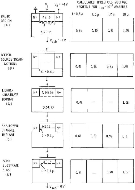
Fig. 10. Threshold voltage calculated using two-dimensional current transport model for various parameter conditions. A flatband voltage of –1.1 V is assumed.
channel threshold [Fig. 10(e)]. The calculations for this ease show appreciably less short-channel effect. In fact the threshold for this case for a device with L = 0.8 µ is about the same as for an L = 1.0 µ device of the basic design. This important improvement is apparently due to the reduced depletion layer widths around the source and drain with the lower voltage drop across those junctions. Also, with these bias and doping conditions, the depletion layer depth in the silicon under the gate is much less at threshold, particularly near the source where only the band bending, ψs, appears across this depiction region, which may help prevent the penetration of field lines from the drain into this region where the device turn-on is controlled.
VIII. CHARACTERISTICS OF THE ZERO SUBSTRATE BIAS DESIGN
Since the last design shown in Fig. 10(e) appears to be better behaved in terms of short-channel effects, it is worthwhile to review its properties more fully. Experimental devices corresponding to this design were built and tested with various channel lengths. In this case a 20 keV. 6.0×10¹¹ atoms/cm2 B11 implant was used to obtain a shallower implanted layer of approximately 1000-Å depth [11]. Data on threshold voltage for these devices with 4 V applied to the drain is presented in Fig. 11 and corresponds very well to the calculated values. Data for a small drain voltage is also given in this figure, showing much less variation of threshold with channel length, as expected. The dependence of threshold voltage on source-to-substrate bias is shown in Fig. 12 for different values of L. The drain-to-source voltage was held at a constant low value for this measurement, The results show that the substrate sensitivity is indeed about the same for this design with zero substrate bias as for the original design with Vsub = –1 V. Note that the smaller devices show a somewhat flatter substrate sensitivity characteristic with relatively lower thresholds at high values of source (and drain) voltage.
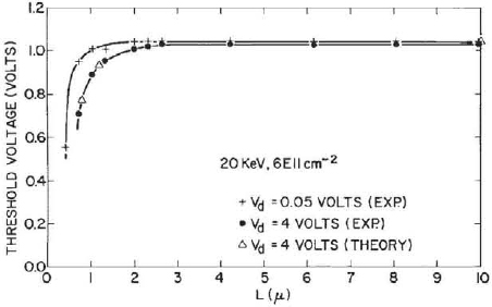
Fig. 11. Experimental and calculated dependence of threshold voltage on channel length for ion-implanted zero substrate bias design.
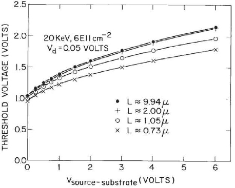
Fig. 12. Substrate sensitivity characteristics for ion-implanted zero substrate bias design with channel length as parameter.
The turn-on characteristics for the zero substrate bias design, both experimental and calculated, are shown in Fig. 13 for different values of L. The relatively small shift in threshold for the short-channel devices is evident: however, the turn-on rate is considerably slower for this ease than for the Vsub = –1 V case shown in Fig. 7. This is due to the fact that the depletion region in the silicon under the gate is very shallow for this zero substrate bias case so that a large portion of a given gate voltage change is dropped across the gate insulator capacitance rather than across the silicon depletion layer capacitance. This is discussed in some detail
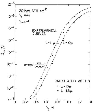
Fig. 13. Calculated and experimental subthreshold turn-on characteristics for ion-implanted zero substrate bias design.
for these devices in another paper [11]. The consequence for dynamic memory applications is that, even though the zero substrate bias design offers improved threshold control for strong inversion, this advantage is offset by the Hatter subthreshold turn-on characteristic. For such applications the noise margin with the turn-on characteristic of Fig. 13 is barely suitable if the device is turned off by bringing its gate to ground. Furthermore, elevated temperature aggravates the situation [18]. Thus, for dynamic memory, the basic design with Vsub = –1 V presented earlier is preferred.
IX. CIRCUIT PERFORMANCE WITH SCALED-DOWN DEVICES
The performance improvement expected from using very small MOSFET’s in integrated circuits of comparably small dimensions is discussed in this section. First, the performance changes due to size reduction alone are obtained from cite scaling considerations given earlier. The influence on the circuit performance due to the structural changes of the ion-implanted design is then discussed.
Table 1 lists the changes in integrated circuit performance which follow from scaling the circuit dimensions, voltages, and substrate doping in the same manner as the device clianges described with respect to Fig. 1. These changes are indicated in terms of the dimensionless scaling factor κ. Justifying these results here in great detail would be tedious, so only a simplified treatment is given, it is argued that all nodal voltages are reduced in the miniaturized circuits in proportion to the reduced supply voltages. This follows because the quiescent voltage levels in digital MOSFET circuits are either the supply levels or some intermediate level given by a voltage divider consisting of two or more devices, and because the resistance V/I of each device is unchanged by scaling. An assumption is made that parasitic resistance elements are either negligible or unchanged by scaling, which will be examined subsequently. The circuits operate properly at lower voltages because the device threshold voltage Vt scales as shown in (2), and furthermore because the tolerance spreads on Vt should be proportionately reduced as well if each parameter in (2) is controlled to the same percentage accuracy. Noise margins are reduced, but at the same time internally generated noise coupling voltages are reduced by the lower signal voltage swings.
Table 1
Scaling Results for Circuit Performance
|
|
|
|
Device or Circuit Parameter |
Scaling Factor |
|
|
|
|
Device dimension tox, L, W Doping concentration Na Voltage V Current I Capacitance εA/t Delay time/circuit VC/I Power dissipation/circuit VI Power density VI/A |
1/κ κ 1/κ 1/κ 1/κ 1/κ 1/κ2 1 |
|
|
|
Due to the reduction in dimensions, all circuit elements (i.e., interconnection lines as well as devices) will have their capacitances reduced by a factor of κ. This occurs because of the reduction by κ2 in the area of these components, which is partially cancelled by the decrease in the electrode spacing by κ due to thinner insulating films and reduced depletion layer widths. These reduced capacitances are driven by the unchanged device resistances V/I giving decreased transition times with a resultant reduction in the delay time of each circuit by a factor of κ. The power dissipation of each circuit is reduced by κ2 due to the reduced voltage and current levels, so the power-delay product is improved by Since the area of a given device or circuit is also reduced by κ2, the power density remains constant. Thus, even if many more circuits are placed on a given integrated circuit chip, the cooling problem is essentially unchanged.
As indicated in Table 2, a number of problems arise from the fact that the cross-sectional area of conductors is decreased by κ2 while the length is decreased only by κ. It is assumed here that the thicknesses of the conductors are necessarily reduced along with the widths because of the more stringent resolution requirements (e.g., on etching, etc.). The conductivity is considered to remain constant which is reasonable for metal films down to very small dimensions (until the mean free path becomes comparable to the thickness), and is also reasonable for degenerately doped semiconducting lines where solid solubility and impurity scattering considerations limit any increase in conductivity. Under these assumptions the resistance of a given line increases directly with the scaling factor κ. The IR drop in such a line is therefore constant (with the decreased current levels), but is κ times greater in comparison to the lower operating voltages. The response time of an unterminated transmission line is characteristically limited
Table 2
Scaling Results for Interconnection Lines
|
|
|
|
Parameter |
Scaling Factor |
|
|
|
|
Line resistance, RL = pL/Wt Normalized voltage drop IRL/V Line response time RLC Line current density I/A |
κ κ l κ |
|
|
|
by its time constant RLC, which is unchanged by scaling; however, this makes it difficult to take advantage of the higher switching speeds inherent in the scaled-down devices when signal propagation over long lines is involved. Also, the current density in a scaled-down conductor is increased by κ, which causes a reliability concern. In conventional MOSFET circuits, these conductivity problems are relatively minor, but they become significant for linewidths of micron dimensions. The problems may be circumvented in high performance circuits by widening the power buses and by avoiding the use of n+ doped lines for signal propagation.
Use of the ion-implanted devices considered in this paper will give similar performance improvement to that of the scaled-down device with κ = 5 given in Table 1. For the implanted devices with the higher operating voltages (4 V instead of 3 V) and higher threshold voltages (0.9 V instead of 0.4 V), the current level will be reduced in proportion to (Vg – Vt)2/tox to about 80 percent of the current in the scaled-down device. The power dissipation per circuit is thus about the same in both cases. All device capacitances are about a factor of two less in the implanted devices. and n+ interconnection lines will show the same improvement due to the lighter substrate doping and decreased junction depth. Some capacitance elements such as metal interconnection lines would be essentially unchanged so that the overall capacitance improvement in a typical circuit would be somewhat less than a factor of two. The delay time per circuit which is proportional to VC/I thus appears to be about the same for the implanted and for the directly sealed-down micron devices shown in Fig. 4.
X. SUMMARY
This paper has considered the design, fabrication, and characterization of very small MOSFET switching devices. These considerations are applicable to highly miniaturized integrated circuits fabricated by high-resolution lithographic techniques such as electron-beam pattern writing. A consistent set of scaling relationships were presented that show how a conventional device can be reduced in size; however, this direct scaling approach leads to sonic challenging technological requirements such as very thin gate insulators. It was then shown how an all ion-implanted structure can be used to overcome these difficulties without sacrificing device area or performance. A two-dimensional current transport model modified for use with ion-implanted structures proved particularly valuable in predicting the relative degree of short-channel effects arising from different device parameter combinations. The general objective of the study was to design an n-channel polysilicon-gate MOSFET with a 1-µ channel length for high-density source-follower circuits such as those used in dynamic memories. The most satisfactory combination of subthreshold turn-on range, threshold control, and substrate sensitivity was achieved by an experimental MOSFET that used a 35 keV, 6.0 × 10¹¹ atoms/cm2 B11 channel implant, a 100 keV, 4 × 10¹⁵ atoms/cm2 As75 source/drain implant, a 350-Å gate insulator, and an applied substrate bias of –1 V. Also presented was an ion-implanted design intended for zero substrate bias that is more attractive from the point of view of threshold control but suffers from an increased subthreshold turn-on range. Finally the sizable performance improvement expected from using very small MOSFET’s in integrated circuits of comparably small dimensions was projected.
APPENDIX
EXPERIMENTAL DETERMINATION OF CHANNEL LENGTH
A technique for determining the effective electrical channel length L for very small MOSFET’s from experimental data is described here. The technique is based on the observation that
![]()
where Rchan is the channel resistance, and pchan the sheet resistance of the channel. For a fixed value of Vg – Vt > 0, and with the device turned on in the below-pinchoff region, the channel sheet resistance is relatively independent of L. Then, a plot of WRchan versus Lmask will intercept the Lmask axis at ΔL because ΔL = Lmask – L, where ΔL is the processing reduction in the mask dimension due to exposure and etching. An example of this technique is illustrated in Fig. 14.
The experimental values of W and Rchan used in Fig. 14 were obtained as follows. First, the sheet resistance of the ion-implanted n+ region was determined using a relatively large four-point probe structure. Knowing the n+ sheet resistance allows us to compute the source and drain resistance Rs and Rd, and to deduce W from the resistance of a long, slender, n+ line. The channel resistance can be calculated from
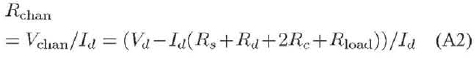
where Rc is the contact resistance of the source or drain, and Rload is the load resistance of the measurement circuit, Id was determined at Vg = Vt + 0.5 V with a small applied drain voltage of 50 or 100 mV. The procedure is more simple and accurate if one uses a set of MOSFET’s having different values of Lmask but all with the same value of
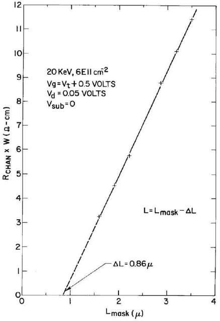
Fig. 14. Illustration of experimental technique used to determine channel length, L.
Wmask. Then one needs only to plot Rchan versus Lmask in order to determine ΔL.
ACKNOWLEDGMENT
We wish to acknowledge the valuable contributions of B. L. Crowder and F. F. Morehead who provided the ion implantations and related design information. Also important were the contributions of P. Hwang and W. Chang to two-dimensional device computations. J. J. Walker and V. DiLonardo assisted with the mask preparation and testing activities. The devices were fabricated by the staff of the silicon technology facility at the T. J. Watson Researeh Center.
REFERENCES
[1] F. Fang, M. Hatzakis, and C. H. Ting, “Electron-beam fabrication of ion implanted high-performance FET circuits,” J. Vac. Sci. Techmol., vol. 10, p. 1082, 1973.
[2] J J. M. Pankrantz, H. T. Yuan, and L. T. Creagh, “A high-gain, low-noise transistor fabricated with electron beam lithography “ in Tech. Dig. Int. Electron Devices Meeting, Dec. 1973, pp. 44–46.
[3] H. N. Yu, R. H. Dennard, T. H. P. Chang, and M. Hatzakis, “An experimental high-density memory array fabricated with electron beam,” in ISSCC Dig. Tech. Papers, Feb. 1973. pp. 98-99.
[4] R. C, Henderson, R. F. W. Pease. A. M. Voshchenkow, P. Mallery, and R. L. Wadsack, “A high speed p-channel random access 1024-bit memory made with electron lithography.” in Tech. Dig. Int. Electron Devices Meeting, Dec. 1973. pp. 138-140.
[5] D. L. Spears and H. L Smith, “X-Ray lithography—a new high resolution replication process,“ Solid State Technol., vol. 15, p. 21. 1972.
[6] S. Middlehoek. “Projection masking, thin photoresist layers and interference effects,” IBM J. Res. Develop., vol. 14, p. 117, 1970.
[7] R. H. Dennard, F. H. Gaensslen, L. Kuhn, and H. N. Yu. “Design of micron MOS switching devices.” presented at the IEEE int. Electron Devices Meeting, Washington, D.C., Dec. 1972.
[8] A. N. Broers and R. H. Dennard. “Impact of electron beam technology on silicon device fabrication.” Semicond. Silicon (Electrochem. Soc. Publication), H. R. Huff and R. R. Burgess, eds., pp. 830–841, 1973.
[9] D. L. Critchlow, R. H. Dennard, and S. E. Schuster, “Design characteristics of n-channel insulated-gate field-effect transistors.” IBM J. Res. Develop., vol. 17, p. 430, 1973.
[10] R. M. Swanson and J. D. Meindl. “Ion-implanted complementary MOS transistors in low-voltage circuits,” IEEE J. Solid-State Circuits, vol. SC-7, pp. 146–153, April 1972.
[11] V. L. Rideout, F. H. Gaensslen, and A. LeBlanc. “Device design considerations for ion implanted n-channel MOSFET’s,” IBM J. Res. Develop., to be published.
[12] F. F. Fang and A. B. Fowler, “Transport properties of electrons in inverted Si surfaces,” Phys. Rev., vol. 169, p. 619, 1968.
[13] W. S. Johnson, IBM System Products Division, E. Fishkill, N.Y., private communication.
[14] H. S. Lee, “An analysis of the threshold voltage for short channel IGFET’s,” Solid-State Electron., vol. 16, p. 1407, 1973.
[15] D. P. Kennedy and P. C. Murley, “Steady state mathematical theory for the insulated gate field effect transistor,” IBM J. Res. Develop., vol. 17, p. 1, 1973.
[16] M. S. Mock, “A two-dimensional mathematical model of the insulated-gate field-effect transistor,” Solid-State Electron., vol. 16, p. 601, 1973.
[17] W. Chang and P. Hwang. IBM System Products Division, Essex Junction, Vt., private communication.
[18] R. R. Troutman, “Subthreshold design considerations for insulated gate field-effect transistors.” IEEE J. Solid-State Circuits. vol. SC-9. p. 55, April 1974.
This page intentionally left blank.


