
As of 2009, the United States accounted for 21 percent of global manufacturing value added, measured at 2009 purchasing-power exchange rates.1 The U.S. share has declined since at least 1990, and the share of producers (including U.S.-owned production facilities) in the industrializing economies in Southeast Asia and elsewhere has grown. Nevertheless, a great deal of cutting-edge innovation and a modest amount of manufacturing activity to support it have remained in the United States, and this generalization applies to photonics and other high-technology industries.
This chapter discusses photonics manufacturing, emphasizing three distinct but closely linked issues. First, it examines the relocation of production of photonics components and products in three key product fields—displays, solar technologies, and optoelectronic components—and the factors behind the offshore movement of much of this production activity. Next, it discusses the relationship between manufacturing and innovation in photonics technologies, highlighting the contrasts and similarities among the three cases in an effort to explain how and where the United States has been able to retain dominance in both production and innovation in selected photonics technologies. Finally, the chapter examines photonics in manufacturing, discussing new advances in manufacturing technologies
_________________
1 United Nations Industrial Development Organization (UNIDO). 2010. International Yearbook of Industrial Statistics. Cheltenham, U.K.: Edward Elgar Publishing.
and production capabilities made possible by applications of photonics technologies.
PRODUCTION AND INNOVATION IN PHOTONICS TECHNOLOGIES: THREE CASE STUDIES
This section presents three case studies—displays, solar cells, and optoelectronics components for the converging communications and computing industry—to examine trends in the offshoring of manufacturing and the relationship between manufacturing and innovation. All three deal with optic and photonic applications based on semiconductor technologies that originated in AT&T Bell Laboratories and other large corporate laboratories. While all three cases have similarities, important differences among them have implications for innovative performance, industry structure, and public policy. It is noteworthy that there is a continued need for increased resolution, smaller features, and increased packing density in all cases of production technologies. This need will drive a need for optical sources and imaging tools supporting the increase in resolution.
Of the three industries, the earliest to move manufacturing overseas from the United States was displays. As discussed by Macher and Mowery in the National Research Council report Innovation in Global Industries: U.S. Firms Competing in a New World,2 although the technological foundations of the display industry were developed in the United States in the 1960s, the industry’s production operations quickly migrated to Japan and then to Korea and Taiwan.3 By 1995, liquid-crystal displays (LCDs) accounted for greater than 95 percent of flat panel display sales by value and thin-film transistor (TFT) LCDs accounted for more than 90 percent of LCD sales, having first found their way into application in calculators, then in cell phones and computers applications, and more recently, as prices continued to decline, largely replacing cathode ray tubes in television receivers.4 Large TFT LCDs accounted for about 75 percent of the value of TFT LCD sales, although the unit production volume of small and medium-size LCDs was five to six times that of large TFT LCDs.5 TFT LCDs remain the dominant display technology.
TFT LCD manufacturing and innovation have their roots in the United States
_________________
2 National Research Council. 2008. Innovation in Global Industries: U.S. Firms Competing in a New World (Collected Studies), J.T. Macher and D.C. Mowery, eds. Washington, D.C.: The National Academies Press.
3 National Research Council. 2008. Innovation in Global Industries.
4 National Research Council. 2008. Innovation in Global Industries.
5 National Research Council. 2008. Innovation in Global Industries.
in the late 1960s with a number of research advances by such major firms as RCA, Westinghouse, Exxon, Xerox, AT&T, and IBM.6 Of those firms, only IBM invested in high-volume manufacturing—through a joint venture with Toshiba in Japan.7 In contrast, all the major Japanese electronics firms invested in high-volume manufacturing. Manufacturers of TFT LCDs face primarily two strategic decisions: when to invest in the construction of a new fabrication facility and whether to move to the next generation of substrates. In 1996, greater than 95 percent of all TFT LCDs were produced in Japan. By 2005, fewer than 11 percent were made in Japan, and the top two production locations were Korea and Taiwan, each of which produced roughly 40 percent of total output. The main reasons for the shift in production location were the lower engineering and labor costs in Korea and Taiwan and the ability of first Korea and then Taiwan to raise the large amounts of capital needed for investing in state-of-the-art fabrication facilities. The window of opportunity for Korean entry occurred in 1991 when Japanese firms were unable to raise the capital needed for investing. Similarly, the window of opportunity for Taiwanese entry came during the Asia crisis of 1997-1998 when Korean firms experienced difficulties in financing new plants.8 (See Figure 7.1.)
Although the successful integration of each generation of production equipment depended on investment in high-volume production, new materials and equipment were not necessarily developed in the same countries that invested in manufacturing. Figure 7.1(b) shows the changing proportion of U.S. versus total U.S. Patent and Trademark Office (USPTO) patents in LCDs. Although it might be tempting to focus on the United States’ declining share of total worldwide LCD patents, it is important to note both that this represents only LCDs, not the next big thing in display technologies, and that even in LCDs the share of patents fails to show a full picture.9 Thus, in addition to IBM’s joint effort with Toshiba for TFT LCD manufacturing, a number of important U.S. firms participated in the industry—most notably, Corning (in substrate materials), Applied Materials (in chemical vapor deposition equipment), and Photon Dynamics (in test, inspection, and repair equipment). These firms remained key players in the market through their ability to acquire knowledge by working collaboratively with manufacturers outside the United States. At the global level, liquid-crystal materials were developed
_________________
6 National Research Council. 2008. Innovation in Global Industries.
7 National Research Council. 2008. Innovation in Global Industries.
8 National Research Council. 2008. Innovation in Global Industries.
9 The data described above are based on the U.S. versus other nations’ shares of patents in the USPTO database. Past research suggests that U.S. patents are a reasonable measure of unique inventive activity worldwide by internationally competitive companies. Notably, the patents described in this data are in no way weighted by their scientific or market value. Thus, there is no way to tell which patents described in Figure 7-1b may be highly incremental additions to existing knowledge rather than revolutionary.
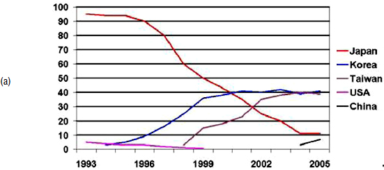
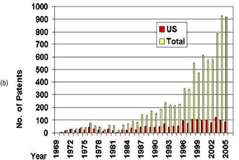
FIGURE 7.1 (a) Percentages of production shares of thin-film transistor (TFT) liquid crystal displays (LCDs). SOURCE: Murtha, T., S.A. Lenway, and J.A. Hart. 2001. Managing New Industry Creation. Stanford, Calif.: Stanford University Press. (b) U.S. firms’ or laboratories’ share of total USPTO LCD patents. SOURCE: U.S. Patent and Trademark Office. 2012. “Patenting in Technology Classes, Breakout by Organization.” Available at http://www.uspto.gov/web/offices/ac/ido/oeip/taf/tecasga/349_tor.htm.
and fabricated primarily in Western Europe and sold to East Asian producers. Chemical vapor deposition equipment was developed primarily in the United States and Western Europe. Testing equipment was developed mainly in Japan and the United States. Finally, lithographic equipment was developed primarily in Japan, the United States, and Western Europe. Given the time pressures created by the frequent transitions from one generation of production technology to the next, materials and equipment suppliers became more important. Unlike their Japanese counterparts, Korean and Taiwanese firms were generally unable to build their own production equipment and instead had to rely largely on external suppliers.10
Although IBM, Corning, Applied Materials, and Photon Dynamics were successful in the display industry, other U.S. firms were less successful. A number of relatively small, niche producers of TFT LCDs engaged in a variety of efforts to catch up with the Japanese, some of which involved financial support from the U.S. government, in particular the Defense Advanced Research Projects Agency (DARPA). Murtha, Lenway, and Hart argue that successful entry by these U.S. firms at this late stage required that they work with partners in East Asia that were experienced in high-volume production.11 U.S. government policies made it difficult for firms receiving government funding to work closely with manufacturers in Asia, and most of these firms did not recognize the importance of collaborating with high-volume manufacturers.12
TFT LCDs dominate today’s display markets, but new market opportunities in displays are opening up particularly in flexible displays. Today, the primary sources of innovation in flexible displays are in the United States, and forecasts suggest that this technology’s market share in mobile devices will grow in the next few years.
As in the case of displays, manufacturing and innovation of solar photovoltaics (PVs) have their roots in the United States. As discussed by Colatat, Vidican, and Lester in the paper Innovation Systems in the Solar Photovoltaic Industry: The Role of Public Research Institutions, the first silicon photovoltaic device was invented in 1954 at Bell Laboratories and found a niche market in space satellites.13 The photovoltaic industry in the 1960s remained very small—the annual market of
_________________
10 National Research Council. 2008. Innovation in Global Industries.
11 Murtha, T.P., S.A. Lenway, and J.A. Hart. 2001. Managing New Industry Creation: Global Knowledge Formation and Entrepreneurship in High Technology—The Race to Commercialize Flat Panel Displays. Stanford, Calif.: Stanford University Press.
12 Murtha et al. 2001. Managing New Industry Creation.
13 Colatat, P., G. Vidican, and R. Lester. 2009. Innovation Systems in the Solar Photovoltaic Industry: The Role of Public Research Institutions. Massachusetts Institute of Technology Industrial Performance Center Working Paper Series. Cambridge, Mass.: Massachusetts Institute of Technology.
solar cells was worth $5 million to $10 million, or the equivalent of 50 to 100 kW of capacity—and the U.S. government was the primary customer.14,15 Throughout the 1950s and 1960s, only five companies produced photovoltaic cells. Two were start-ups: Hoffman Electronics, which acquired National Fabricated Products and its patent license for the Bell Laboratories patents, and Heliotek, founded by Alfred Mann as a spin-off from his previously founded company, Spectrolab.16 The remaining three entrants were established companies that had diversified into the solar cell market: RCA (which produced radios), International Rectifier (which produced semiconductors), and Texas Instruments (which produced semiconductors). All three of the established companies left the market by the end of the 1960s because it was small and unpredictable.17
In 1973, the Arab oil embargo strengthened interest in terrestrial applications of photovoltaics and expanded the market for them.18 Two well-known U.S. PV firms were founded shortly thereafter by former employees of Spectrolab: Solar Technology International (1975) and Solec International (1976).19,20 Between the mid-1980s and the mid-1990s, the United States, Japan, and Germany competed for the lead in solar cell production on the basis of the location of production activities. In the mid-1980s, Japan overtook the United States as the number one producer of solar cell modules, with Germany in a distant third place. The United States and Germany then surpassed Japan in world PV module shipments in the mid-1990s. Since the 1995, however, although U.S. production of PVs has risen, the U.S. share of global PV production has fallen from its 43 percent peak in 1995 to an all-time low of 6 percent in 2009.21 (See Figure 7.2 (b).) As of 2009, Germany is the leader
_________________
14 Colatat et al. 2009. Innovation Systems in the Solar Photovoltaic Industry.
15 National Research Council. 1972. Solar Cells: Outlook for Improved Efficiency. Washington D.C.: National Academy Press.
16 Colatat et al. 2009. Innovation Systems in the Solar Photovoltaic Industry.
17 Colatat et al. 2009. Innovation Systems in the Solar Photovoltaic Industry.
18 Colatat et al. 2009. Innovation Systems in the Solar Photovoltaic Industry.
19 Colatat et al. 2009. Innovation Systems in the Solar Photovoltaic Industry.
20 Although both firms are still in operation, both were eventually acquired by non-U.S. companies. Solar Technology International was acquired by Atlantic Richfield Company (ARCO) in 1977 and renamed ARCO Solar. By the time it was acquired by Siemens (a German company) in 1990, ARCO Solar was the largest PV manufacturer in the world. ARCO Solar was later sold by Siemens to an Anglo-Dutch company, Shell, before being sold to Solarworld (a German company). Solec International, which was eventually sold to Sanyo (a Japanese company), is also still in operation today.
21 Le, Minh, Chief Engineer, Solar Energy Technologies Program, U.S. Department of Energy. 2011. “The SunShot Program—The Great Solar Race: The Apollo Mission of Our Times.” Presentation to the NRC Committee on Harnessing Light: Capitalizing on Optical Science Trends and Challenges for Future Research, February 24, 2011.
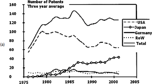
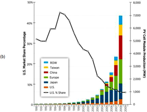
FIGURE 7.2 (a) U.S. share of global patenting. SOURCE: Reprinted, with permission, from Andersson, B.A., and S. Jacobsson. 2000. Monitoring and assessing technology choice: The case of solar cells. Energy Policy 28(2000):1037-1049. (b) U.S. share of global PV cell module market and production. SOURCE: Le, Minh, Chief Engineer, Solar Energy Technologies Program, U.S. Department of Energy. 2011. “The SunShot Program—The Great Solar Race: The Apollo Mission of our Times.” Presentation to the NRC Committee on Harnessing Light: Capitalizing on Optical Science Trends and Challenges for Future Research, February 24, 2011.
in global production of PV followed by China, with Japan in third place.22 But the growth of international production means that three of the top five manufacturers of PV modules (measured in megawatts of shipments23) in 2010 were Chinese. The firm in second place on the basis of its volume (megawatts) of shipments at the end of the fourth quarter of 2010 is First Solar, a U.S. thin-film PV company that uses cadmium telluride instead of silicon (the material used by all 9 other companies in the top 10) as its semiconductor. First Solar has manufacturing facilities in Perrysburg, Ohio; Frankfurt, Germany; and Kulim, Malaysia. There are no other U.S. companies in the top 10. The Japanese company Sharp is in fourth place, and a Canadian company, Canadian Solar, is in sixth place. The top 10 manufacturers accounted for more than 50 percent of total global PV shipments in 2010.24
Although the United States no longer dominates global production of solar modules, it has maintained its lead in patenting in solar technologies,25 followed by Japan (according to the geographic location reported by the corporate assignees on the patent). As can be seen in Figure 7.2, the United States was the dominant source of solar technology patents during 1975-1995, although Japan’s share of global patenting increased significantly after 1980.26 The United States retains a position of leadership in solar-related USPTO patents, accounting for 52 percent of total solar patents in 2002-2010, followed by Japan at 26 percent and Germany at 6 percent.27 The 10 leading corporate patentees during 2002-2010 were (in order) Canon (Japanese), Sharp (Japanese), Boeing (U.S.), Sunpower (U.S.), Kanegafuchi (Japanese), Sanyo (Japanese), Emcore (U.S.), Applied Materials (U.S.), Konarka (U.S.), and Rabinowitz (U.S.).28
As this discussion suggests, the United States no longer is among the leading
_________________
22 Le, Minh, Chief Engineer, Solar Energy Technologies Program, U.S. Department of Energy. 2011. “The SunShot Program—The Great Solar Race: The Apollo Mission of Our Times.” Presentation to the NRC Committee on Harnessing Light: Capitalizing on Optical Science Trends and Challenges for Future Research, February 24, 2011.
23 The conditions for measuring the nominal power of a photovoltaic module are specified in standards such as IEC 61215, IEC 61646, and UL 1703; the term “power” is also used in describing the size of a shipment or an installation.
24PVinsights. 2011. “Suntech Lost Championship of Solar Module Shipment to First Solar in 2Q11.” Available at http://pvinsights.com/Report/ReportPMM31A.php. Accessed December 27, 2011.
25 The above-described data are based on shares of patents in the U.S. Patent and Trademark Office database. Past research suggests that U.S. patents are a reasonable measure of unique inventive activity worldwide by internationally competitive companies. Here, patent locations are assigned on the basis of company assignee location, as reported in the filed patent.
26 Andersson, B.A. and S. Jacobsson. 2000. Monitoring and assessing technology choice: The case of solar cells. Energy Policy 28(14):1037-1049.
27 Cardona, V. 2011. “Clean Energy Patents—Winners and Losers, Renewable Energy World.” Available at http://www.renewableenergyworld.com/rea/news/print/article/2011/03/2010-clean-energy-patents-winners-and-losers. Accessed July 5, 2011.
28 Cardona, V. 2011. “Clean Energy Patents—Winners and Losers, Renewable Energy World.”
sites (by volume) for the manufacturing of solar modules.29 Notable is the apparent lack of correlation between the nations in which the bulk of solar module manufacturing is sited and the nations that dominate inventive activity (as measured by USPTO patenting). (See Figure 7.2 (b).) Indeed, the United States continues to dominate global inventive activity in solar technologies despite not being the location for the greatest volume of solar module manufacturing output. (See Figure 7.2 (a).) Notably, the largest volume in the world of patents is in cutting-edge solar technologies, such as thin films, which are still produced largely in the United States. In contrast, the largest volume of manufacturing is in crystalline silicon technology modules—a technical field that no longer dominates solar technology patenting in the USPTO.
Innovation in the materials that underpin solar technologies used for energy generation may prove important in affecting the future site of manufacturing activity in this field. Numerous materials and designs can produce photovoltaic effects.30 Overall, PV technologies can be grouped into four main categories: wafer and thin film (including crystalline and amorphous silicon and cadmium telluride technologies), concentrator, excitonic (including organic polymer and dye-sensitized solar technologies), and novel, high-efficiency technologies (such as plasmonics).31 Designs based on crystalline silicon have dominated commercial PV technology, accounting for more than 80 percent of the market for commercial modules since the industry’s origin.32 Crystalline silicon may not, however, be the future. Today, thin-film solar technologies hold the second-largest proportion of the commercial market after crystalline silicon, hovering below 20 percent.33 In the 1980s, both the United States and Japan invested in thin-film amorphous silicon technologies.34 One report finds that between 1994 and 1998 the number of USPTO patents granted in amorphous silicon exceeded the number granted in crystalline silicon.35 A more recent report based on National Renewable Energy Laboratory data concluded that the cost per watt of producing thin-film PV was closing the gap with the cost of producing crystalline PV in the late 1990s and early
_________________
29 At the firm level, one U.S.-headquartered firm is among the corporate leaders (by volume) in global manufacturing of solar modules. However, the national headquarters of the corporate entities that dominate solar manufacturing may not correlate with the geographic location of those corporations’ manufacturing activities.
30 Baumann, A., Y. Bhargava, Z.X. Liu, G. Nemet, and J. Wilcox. 2004. Photovoltaic Technology Review. Berkeley, Calif.: University of California, Berkeley.
31 Curtright, A.E., M.G. Morgan, and D. Keith. 2008. Expert assessment of future photovoltaic technology. Environmental Science and Technology 42(24): 9031-9038.
32 Baumann et al. 2004. Photovoltaic Technology Review.
33PVinsights. 2011. “Suntech Lost Championship of Solar Module Shipment to First Solar in 2Q11.” Available at http://pvinsights.com/Report/ReportPMM31A.php. Accessed December 27, 2011.
34 Baumann et al. 2004. Photovoltaic Technology Review.
35 Andersson and Jacobsson. 2000. Monitoring and assessing technology choice.
2000s.36 However, even in-depth assessments find it difficult to assess which of the thin-film or the many other PV material and design technologies may be dominant in the future.37 Inasmuch as the basic materials underpinning solar technologies are likely to undergo considerable change, it is possible that U.S.-based innovation can lead to expanded U.S.-based production of new technologies in this field.
Optoelectronic Components for Communications Systems
Optoelectronic components—which include lasers, modulators, amplifiers, photodetectors, and waveguides produced on semiconductors—are the components necessary to send and receive information in light-based communications systems. The origins of this technology can be traced to the 1960 demonstration of the laser at Hughes Aircraft that followed from research at Columbia University and AT&T Bell Laboratories (see Chapter 2 for further discussion). Further research and development (R&D), much of it at Bell Laboratories, yielded the fabrication methods by which fiber and the other system-critical optoelectronic components could be manufactured economically. In 1970, Corning was the first firm to develop the optical waveguide technology—in particular, low-loss optical fiber that would prove critical to the development of optoelectronics. Corning entered into joint-development cross-licensing agreements with AT&T and cable suppliers in Europe and Japan. By 1986, several other giant corporations had begun production of fiber optics and related components, including DuPont, ITT, Allied Signal, Eastman Kodak, IBM, and Celanese. Large Japanese corporations, including Nippon Electric Company, made similar investments.38
The 1984 consent decree that resolved the federal antitrust suit against AT&T produced dramatic changes in the structure of R&D and manufacturing in the U.S. communications industry, and these changes affected the development of optoelectronics in the United States. In 1996, AT&T spun off Bell Laboratories with most of its equipment manufacturing business into a new company named Lucent Technologies. In 2006, Lucent signed a merger agreement with the French company Alcatel to form Alcatel-Lucent. On August 28, 2008, Alcatel-Lucent announced that it was pulling out of basic science, material physics, and semiconductor research to work in more immediately marketable fields.39
During the 1990s, many small and medium-size optoelectronic component
_________________
36 Baumann et al. 2004. Photovoltaic Technology Review.
37 Curtright et al. 2008. Expert assessment of future photovoltaic technology.
38 Sternberg, E. 1992. Photonic Technology and Industrial Policy: U.S. Responses to Technological Change. Albany, N.Y.: State University of New York Press.
39 Ganapati, Priya. 2008. Bell Labs kills fundamental physics research. Wired Magazine. August 27. Available at http://www.wired.com/gadgetlab/2008/08/bell-labs-kills/. Accessed November 12, 2012.
manufacturers for communications were founded in the United States.40 In March 2000, however, the telecommunications bubble burst, throwing the industry into turmoil. By 2002, optical fiber sales had fallen short of monthly projections by more than 80 percent,41 and competitive survival of producers of fiber and components required that they reduce production costs rather than develop novel technologies.42
The collapse of the U.S. telecommunications equipment market led to dramatic change in the location of optical components production. Between 2000 and 2006, the majority of optoelectronic component manufacturers moved manufacturing activities from the United States to developing countries, in particular to developing East Asia.43 By 2005, five U.S.-based companies (Agilent Technologies, JDSUniphase, Bookham, Finisar, and Infineon) and two Japanese-based companies (Mitsubishi and Sumitomo Electric/ExceLight) accounted for 65 percent of revenues in optoelectronic components.44 All five of the top U.S. manufacturers had moved assembly activities to East Asia, and all but JDSUniphase had also moved some or all of their fabrication activities to East Asia. The offshore production activities of these U.S. firms did not rely on contract manufacturers, instead producing components in wholly owned foreign subsidiaries. Only a few U.S. entities, mainly start-ups relying on funding from venture capitalists or Small Business Innovation Research (SBIR), chose to keep all manufacturing in the United States. Included among these start-ups were Infinera, Kotura, and Luxtera.
Despite these changes in the location of manufacturing, as can be seen in Figure 7.3, the United States has maintained a dominant role in total optoelectronics patent production as measured by USPTO data, with Japan a close second. In the 4-year period (2001-2004) after the bursting of the telecommunications and Internet bubble, U.S. patents filed annually by assignees in the United States fell while U.S. patenting during the same period by assignees in Japan continued to rise.
Although those data depict trends in issued patents, which have to pass a formal review for novelty and non-obviousness by USPTO examiners, they do not adjust for the fact that the economic or technological importance of individual patents varies widely. Nor do these patent data indicate the location of the inventive activity
_________________
40 Yang, C., Nugent, R., and Fuchs, E. 2011. Gains from Other’s Losses: Technology Trajectories and the Global Division of Firms. Carnegie Mellon University Working Paper. Available at http://papers.ssrn.com/sol3/papers.cfm?abstract_id=2080595. Accessed November 12, 2012.
41 Fuchs, E.R.H., E.J. Bruce, R.J. Ram, and R.E. Kirchain. 2006. Process-based cost modeling of photonics manufacture: The cost competitiveness of monolithic integration of a 1550-nm DFB laser and an electroabsorptive modulator on an InP platform. Journal of Lightwave Technology 24(8):3175-3186.
42 Fuchs et al. 2006. Process-based cost modeling of photonics manufacture.
43 Yang et al. 2011. Gains from Other’s Losses.
44 Fuchs et al. 2006. Process-based cost modeling of photonics manufacture.
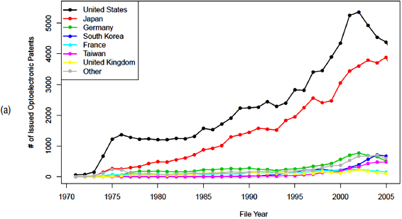
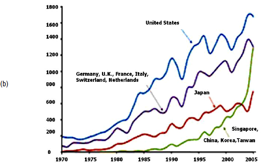
FIGURE 7.3 (a) The United States and Japan dominate U.S. Patent and Trademark Office (USPTO) patents in optoelectronics. NOTE: Country assigned by patent assignee’s filed location. SOURCE: Reprinted, with permission, from Ventura, S., R. Nugent, and E. Fuchs. 2012. Methods Matter: Revamping Inventor Disambiguation Algorithms with Classification Models and Labeled Inventor Records. Working paper. Abstract available at http://ssrn.com/abstract=2079330. (b) Optoelectronic publications of some major countries (1970-2005). Historically, the United States dominates publications in optoelectronics, followed by Japan and then various countries in Europe; in recent years, however, publication rates from East Asia have risen dramatically. SOURCE: Reprinted, with permission, from Doutriaux, T., 2009. “The Resiliency of the Innovation Ecosystem: The Impact of Offshoring on Firms Versus Individual Technology Trajectories.” Work toward a master’s thesis. Advisor: E. Fuchs. Pittsburgh, Pa.: Carnegie Mellon University.
that led to the patents that were issued in the United States. The trends in patenting thus provide some information on the location of inventive activity, but they also reflect inventor (or assigned) perceptions about the location of market opportunities for the exploitation of the inventions. And the United States retains a dominant position as a focus of global patenting activity in optoelectronics.
Publication records covering the 1970-2005 period in optoelectronic components reveal a slightly different picture. For the first three decades of this period, the United States accounts for the largest number of publications, followed by key countries in Europe and Japan. Since roughly 2000, however, an almost exponential rise can be seen in publications from developing East Asia as the total number of publications from China, Korea, Taiwan, and Singapore surpassed the total number of publications from Japan by 2003 and reached parity with the number of publications from Germany, France, Italy, the Netherlands, Switzerland, and the United Kingdom by 2005. Those publication data are not normalized for quality and therefore can be best interpreted as measures of overall research activity in optoelectronics within each country, in contrast with the patent data described above. Arguably, the publications data indicate a significant rise in optoelectronics research activity in the industrializing economies of East Asia since 2000.
To elucidate the relationship between manufacturing location and the rate and direction of innovation in optoelectronic components better, the following discussion addresses the technical details of the innovations that U.S. optoelectronic component manufacturers were pursuing when they began to move their production activities offshore. As was true of the electronics industry 30 years ago, three competing design technologies are used in optoelectronic components. Older, more established designs use discrete components that are wire-bonded together. The most recent designs, however, rely on the capability to do “monolithic integration”—the fabrication and integration (using semiconductor techniques) of multiple functions on a single chip. Between those extremes are designs that use intermediary “hybrid integration” techniques with a variety of methods to bond components to one another. Monolithic integration holds considerable promise for product innovation in the photonics industry, because it significantly reduces size, packing alignment, complexity, and cost while potentially improving the reliability of photonic components, thereby enabling their application to markets outside telecommunications, such as computer chips (especially optical buses), biosensors, and other small-scale sensing and information processing applications.45
During the 1980s and 1990s, when optoelectronics was being used extensively
_________________
45 Akinsanmi, W., R. Reagans, and E.R.H. Fuchs. 2011. Economic Downturns, Technology Trajectories, and the Careers of Scientists. Presented June 2 at Atlanta Conference on Science and Innovation Policy. Available at http://smartech.gatech.edu/bitstream/handle/1853/42529/527-1641-1-PB.docx?sequence=1. Accessed November 12, 2012.
in telecommunications, an optoelectronic firm’s competitiveness depended on the speed with which it could bring the latest innovations to market.46 During that period, firms manufacturing optoelectronics components for applications in telecommunications focused their process-technology development on monolithic integration (Figure 7.4) to improve component reliability and reduce cost.47 The transfer by many U.S. optoelectronic component manufacturers of their assembly and fabrication activities offshore after the bursting of the telecommunications bubble shifted their focus in process innovation away from monolithic integration to discrete-technology solutions. That shift largely reflected the different manufacturing-cost environment of the 1990s in the industrializing East Asian economies within which the U.S. firms were operating their offshore facilities and the shift in the competitive environment to favor low-cost production over rapid introduction of new component designs.48
Those firms found that the lowest-cost option was to manufacture the discrete technologies in developing countries and abandon U.S. production of monolithically integrated technologies.49 It is not clear, however, that the apparent declines in monolithic-integration patenting in the firms that have moved production activities offshore will necessarily lead to a decline in overall innovation by U.S. firms in monolithic integration. Several start-up firms that focus on monolithic-integration technologies have emerged in the United States since 2000. It is also possible that established U.S. optoelectronic component manufacturers that have kept fabrication in the United States will increase R&D and patenting in monolithic integration for optoelectronics. Finally, and perhaps most important, firms outside telecommunications and data communications, such as computing firms, may find it in their interest to develop monolithic-integration design and fabrication capabilities for communications applications, as evidenced by Intel’s recent establishment of a silicon photonics design and fabrication facility at the University of Washington.
The case of optoelectronics components illustrates a strong relationship between the location of production activities by U.S. firms and the direction of these firms’ innovative efforts. But the evidence presented in this case suggests that the movement of optoelectronics-component production to non-U.S. locations has thus far not resulted in the “loss” by the U.S. economy of innovative capabilities
_________________
46 Fuchs, E.R.H., and R.E. Kirchain. 2010. Design for location: The impact of manufacturing offshore on technology competitiveness in the optoelectronics industry. Management Science 56(12):2323-2349.
47 Fuchs et al. 2010. Design for location.
48 Yang et al. 2011. Gains from Other’s Losses.
49 Recent research shows that moving assembly activities offshore is associated with a decrease in monolithic integration patenting activities, although overall patenting other than monolithic integration increases. U.S. firms that move both assembly and fabrication activities offshore, however, display declines in all optoelectronics patenting. Yang et al. 2011. Gains from Other’s Losses.
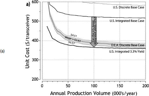
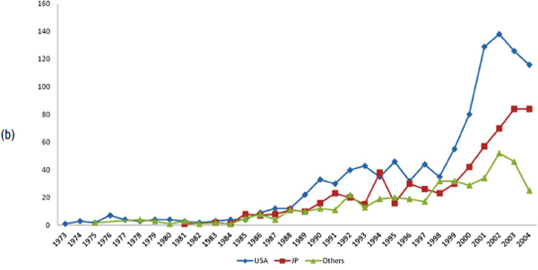
FIGURE 7.4 (a) U.S. monolithically integrated design produced in the United States cannot cost-compete with the discrete design produced in developing East Asia (D.E.A.). SOURCE: Reprinted, with permission, from Fuchs, E., and R. Kirchain. 2010. Design for location: The impact of manufacturing offshore on technology competitiveness in the optoelectronics industry. Management Science 56(12):2323-2349. (b) U.S. firms maintain cumulative dominance in USPTO patents in optoelectronic integration; however, Japanese firms have equal or higher numbers of patents in some years. SOURCE: Reprinted, with permission, from Yang, C., R. Nugent, and E. Fuchs. 2011. Gains from Others’ Losses: Technology Trajectories and the Global Division of Firms. Carnegie Mellon University Working Paper. Available at http://papers.ssrn.com/sol3/papers.cfm?abstract_id=2080595.
in monolithic integration. Instead, the committee observes that a different set of U.S. corporations (and universities) now have become active in this technological field.50,51
Similarities and Differences Among the Three Cases
The displays, solar, and optoelectronic communications components cases demonstrate important similarities and differences. All three cases involve semiconductor processing technologies in which R&D and manufacturing activities are linked. In all three, technologies originated in the 1950s and 1960s in corporate R&D laboratories in the United States—for example, AT&T Bell Laboratories, IBM, and Corning. In all three cases, manufacturing (often in U.S.-owned facilities) has moved overseas and the United States has lost its position as the leading site for production activities. In the case of displays, manufacturing moved first to Japan, then to Korea and then Taiwan. In the case of solar, the dominant site of manufacturing moved to Germany and China. In the case of optoelectronic components for communication systems, the dominant manufacturing position moved to developing East Asia.
In all of those cases, manufacturing moved overseas, but the primary offshore manufacturing site did not always become the leading source of innovation. Indeed, in all three cases, U.S.-based firms and inventors are leading technological advances, at least some of which could displace established and dominant producers. The potentially disruptive technologies include flexible displays, thin-film and other technologies in the solar field, and monolithically integrated design and fabrication technologies in optoelectronic communications systems.
In contrast with the pattern of innovation, entry, and early-stage growth of many of these technologies in the 1950s and 1960s, the new technological possibilities are being pursued by start-up firms, often in collaboration with U.S. government laboratories or universities (see Figure 7.5, which shows the growing role of U.S. universities in optoelectronics patenting). Moreover, the U.S. defense market often is a less central source of demand for innovative technologies. The new approach to technology development that relies more heavily on universities and small and medium-size firms for innovation, in which venture-capital funding plays a more important role, may increase the importance of mechanisms to support cross-industry and cross-institutional coordination in helping the United States to maintain leadership in photonics innovation.
The three cases also highlight important differences among the technologies. In displays and optoelectronic components, the vast majority of manufacturing has
_________________
50 Akinsanmi et al. 2011. Economic Downturns, Technology Trajectories, and the Careers of Scientists.
51 Yang et al. 2011. Gains from Other’s Losses.
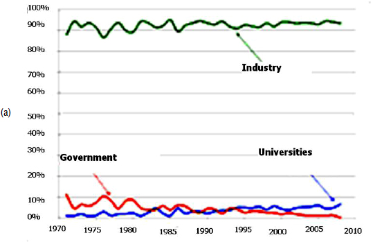
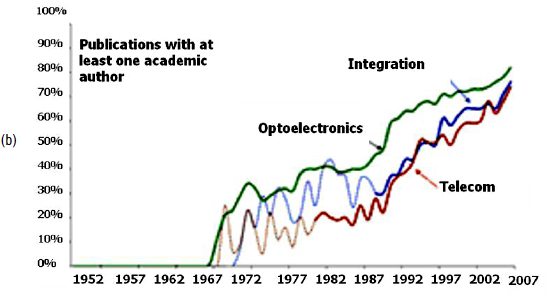
FIGURE 7.5 The institutional locus of innovation in optics. An example from optoelectronic components for the communications industry. (a) Over the last nearly four decades, firms have remained the predominant source of U.S. Patent and Trademark Office patents in optoelectronics. NOTE: The industry, government, or university label is according to patent assignee. (b) Over the last four decades, universities have contributed to a growing percentage of optoelectronic publications. SOURCE: Reprinted, with permission, from Doutriaux, T. 2009. “The Resiliency of the Innovation Ecosystem: The Impact of Offshoring on Firms Versus Individual Technology Trajectories.” Work toward a master’s thesis. Advisor: E. Fuchs. Pittsburgh, Pa.: Carnegie Mellon University.
moved to developing countries where labor and engineering are cheaper. In solar, however, the leading producer, Germany, is a developed country in which direct-line and engineering wages are as high as or higher than those in the United States.
The close tie between R&D and manufacturing also has different consequences in the three cases. In the case of displays, the close tie led U.S. firms to collaborate with foreign manufacturers to remain at the cutting edge of innovation. In the case of solar, the close tie between R&D and manufacturing means that R&D occurs largely in the same country as manufacturing and has enabled U.S.-based R&D and manufacturing of thin-film technologies to remain dominant. Finally, in the case of optoelectronic components for communications systems, the close tie between R&D and manufacturing led firms that moved manufacturing overseas to abandon monolithically integrated technologies. As a result, monolithic integration continues to be dominated by private firms that remain in the United States.
Those differences yield different policy implications for each industry. In the case of displays, government policies preventing firms from collaborating with foreign enterprises (such as might exist as stipulations for certain work with the Department of Defense [DOD] could have a negative impact on innovation. In the case of solar, the dominant position of German-based production suggests that developing countries may not be the site for cost-competitive manufacturing. The dominance of patenting and production in thin-film technologies by U.S.-based firms suggests that the United States may have the opportunity to be a leader not only in innovating but also in the next generation of advanced solar manufacturing. Finally, in the case of optoelectronic components for communications systems, government and venture funding of small and medium-size enterprises pursuing next-generation monolithically integrated technologies may be critical to overcome the gap between current market demands and longer-term markets in computing and biotechnology that may require the low-power and smaller form-factor performance offered by monolithically integrated solutions. Those differences highlight the importance of avoiding a single-blanket policy for all of photonics. Instead, it is essential to engage technical and industry experts in policy development to exploit their contextual understanding of implications and possible outcomes.
ADVANCED MANUFACTURING IN OPTICS
This section discusses advances in manufacturing technologies in optical component and optical systems production, which have experienced considerable progress over the last decade. Technologies that were considered innovative a dozen years ago have undergone significant evolution and are now found in operation in many optics manufacturing firms. Improvements in generation, finishing, assembly, and metrology technologies are being leveraged to generate higher-performing optical systems and push the upper end of the precision scale. Many of these systems
include aspherical lenses, which have advantages over spherical lenses but are more difficult to produce. This section briefly describes the advantages of aspherical lenses and then addresses some of the recent improvements in their production (for a much more detailed description, see Appendix C). The push toward the upper end of the precision scale will drive the need for improvements in optical sources and imaging tools to support the increase in resolution.
Spherical lenses have been the workhorse of optical systems for centuries. The curved surfaces of a lens cause rays of light from a point on a distant object to come to a focus. A single lens with spherical surfaces forms an image that is not a perfect point. (See Figure 7.6.) Optical design has traditionally been a search for combinations of spherical-surfaced components.
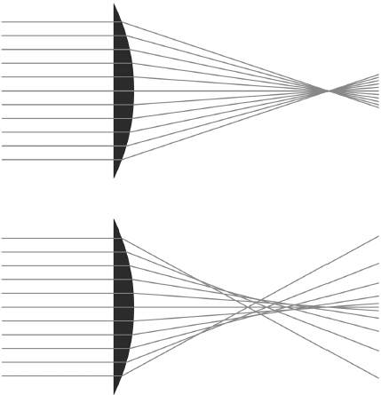
FIGURE 7.6 Light rays are focused to a single focal point with an ideal lens (top). A lens with a spherical surface has an associated spherical aberration, and therefore has no distinct focal point (bottom). (Image is exaggerated).
Spherical components are relatively inexpensive, partly because of improvements in lapping processes that allow the simultaneous processing of multiple lenses. Although time-consuming, lapping is capable of producing high-quality polished surfaces that deviate from the designer’s specifications by as little as a few hundredths of a wavelength. The result is high-precision, cost-effective lenses.
Aspherical lenses allow an expansion in the optical designer’s solution set. In an aspherical lens, the surfaces can be nonspherical. The addition of high-order curvature to an otherwise spherical surface in an aspherical lens permits independent correction or balancing of spherical aberration. That leads to a reduction in the number of lens surfaces needed for aberration-corrected imagery.
Because they can reduce lens surfaces, the use of aspherical lenses can improve transmission and reduce the weight, space requirements, and cost of optical systems. Although their potential for improving performance of an optical design had been known for many years, their use had been limited by the inability to produce them reliably and accurately. Advances in manufacturing process technologies—including deterministic computer numerically controlled (CNC) manufacturing equipment and processes, single-point diamond turning and grinding, polymer molding, glass molding, and precision metrology—have made possible the manufacture and use of these important surface geometries.52 Among the diverse applications of high-precision aspheric lenses (aspheres) are military aerospace systems, optical data storage, photolithography, and astronomy. Lower-precision aspheres have a wider range of application, including photography and video imaging (especially zoom lenses), such medical instruments as endoscopes, telecommunications, and document scanners and printers. At the low end of the market, aspheres find use in such applications as condenser elements for illumination. Asymmetrical aspheres are also becoming important, especially in conformal applications, in which the outer surface of an optical component must conform to the aerodynamic shape of an aircraft or missile.
Fabrication Processes and Equipment
Processes and equipment available to fabricate optical surfaces, particularly aspherical surfaces, have undergone notable improvement during the last decade. Improvements have been made in both the ability to produce and the ability to measure precision optical components. Improvement has included nearly all aspects
_________________
52 For more information on the techniques discussed in this section, see Appendix C of this report.
of fabrication from surface generation to coating and the ability to measure these surfaces.
Today, CNC grinding and polishing allow dynamically adjustable cutting paths for tool wear and can be programmed for edging, beveling, sagging, concave, and convex surface grinds. Polymer molding has also become common in fabrication of lenses for consumer and commercial products. Mobile phones, DVD players, digital cameras, and conferencing systems have all incorporated polymer lenses. Glass-molding technology also has become increasingly available in the last decade, as has magnetorheological finishing (MRF) in the fabrication of optical components. In MRF, ferrous-laden fluid passes through an electromagnetic field, where its viscosity is increased, allowing the creation of a precise and repeatable polishing tool. Single-point diamond turning (SPDT) has also grown in popularity in fabricating optical components. It is now routinely used to produce mold inserts for polymer lenses, mold inserts for glass molding, and finished optical elements. The machining process uses single-crystal diamond cutting tools and nanometer-precision positioning to generate spherical surface geometries and more complex geometries, such as toroids, aspheres, and diffractives.
Optical thin-film coatings technology has advanced in response to requirements in diverse markets, including telecommunications, health and medicine, biometrics, and defense. Evaporation deposition processes, in which materials are deposited by way of a transformation from solid to vapor and back to solid, are the most widely used in the optics industry in spite of problems stemming from the porosity of coatings and their sensitivity to humidity and thermal conditions. Metrology is an important enabling technology in the optics industry. There is an old saying, “If you can’t measure it, you can’t make it;” over the last decade, advances in interferometry have improved the ability to measure increasingly challenging optics, particularly aspheres.53,54,55
APPLICATIONS OF PHOTONICS IN MANUFACTURING
This section discusses photonics-enabled advances in process technologies with potentially broad applications in numerous manufacturing industries. As noted below, many of these process-technology innovations hold considerable potential
_________________
53 PalDey, S., and S.C. Deevi. 2003. Single layer and multilayer wear resistant coatings of (Ti,Al)N: A review. Materials Science and Engineering A 342(1-2):58-79.
54 Kelly, P.J., and R.D. Arnell. 2000. Magnetron sputtering: A review of recent developments and applications. Vacuum 56:159-172.
55 Svedberg, E.B., J. Birch, I. Ivanov, E.P. Munger, and J.E. Sundgren. 1998. Asymmetric interface broadening in epitaxial Mo/W (001) superlattices grown by magnetron sputtering. Journal of Vacuum Science and Technology A: Vacuum, Surfaces, and Films 16(2):633-638.
to enable the United States to retain manufacturing capability in the face of intensifying international competition.
For the last several decades, photolithography has been the dominant printing technology used by integrated circuit (IC) manufacturers, and it is a key factor in increasing the transistor density per silicon area and lowering the cost per transistor as described by Moore’s law.56 It has played an important role in fabricating high-volume ICs, microelectromechanical systems (MEMS), and other microdevices and nanodevices. Since the publication of the National Research Council report Harnessing Light: Optical Science and Engineering for the 21st Century, photolithography in IC manufacturing has remained dominant and has continued to achieve impressive technical advances.
Photolithography is similar to photography in that both use imaging optics and a photosensitive film to record an image. In photolithography, the surface of a semiconductor wafer is coated with a light-sensitive polymer known as a photoresist. Light passing through a mask that contains the desired pattern is focused on the photoresist-coated wafer. The material properties of a photoresist change when it is exposed to light, and the changed material can be selectively removed from the wafer surface. The wafer is then chemically treated to engrave (etch) the exposure pattern in it. The process is repeated many times with different masks to form billions of complicated three-dimensional structures (such as transistors and interconnections) on the wafer. A generic lithographic process is schematically shown in Figure 7.7.
Photolithography has enabled manufacturers to increase transistor density (and thus the complexity of advanced chips) while lowering the cost per transistor; historically, the cost per transistor has decreased by close to 30 percent per year. An important aspect in the advancement of photolithography is the minimum feature size (resolution) provided by the optical projection system that projects the mask image onto the wafer. The minimum feature size is generally formulated by the Rayleigh scaling equation and is directly related to λ, the exposure wavelength, and inversely related to the numerical aperture (NA) of the projection optics, by k1, a scaling constant that is a function of the process, the photoresist, the type of feature being printed, and other factors. From Rayleigh’s equation, resolution can
_________________
56 Brunner, T.A. 2003. Why optical lithography will live forever. Journal of Vacuum Science and Technology B 21(6):2632-2637.
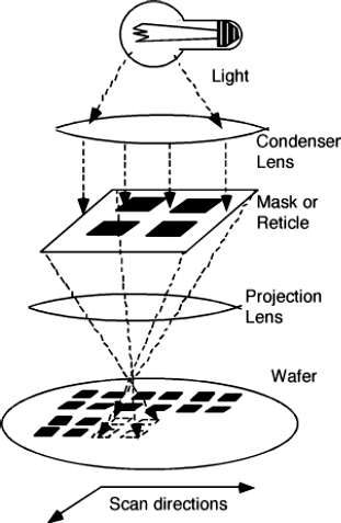
FIGURE 7.7 Generic schematic diagram of the lithographic process. SOURCE: Bill Wilson. 2007. “Photolithography.” Connexions. Available at http://cnx.org/content/m1037/2.10/. Reprinted with permission.
be improved by (1) reducing the wavelength of the light source, (2) increasing the NA of the lens, and (3) decreasing the value of k1.57
One common approach to reducing the feature size is to reduce the wavelength of light. In the early days of photolithography, the mercury arc lamp “G-line” optical source with a wavelength of 436 nm was used; this resulted in a feature size down to about 700 nm. The transition to “I-line” sources at a 365-nm wavelength enabled resolution below 400 nm, and the use of KrF excimer lasers at a 248-nm wavelength
_________________
57 Mack, C.A. 2007. Fundamental Principles of Optical Lithography: The Science of Microfabrication. Hoboken, N.J.: Wiley.
allowed resolution down to 150 nm. Current state-of-the-art lithography technology uses light with a 193-nm wavelength to fabricate feature sizes below 32 nm.
Feature size could also be reduced by increasing the NA of the projection system. The first projection lithography tools had an NA of 0.16 in 1973, and the NA has steadily increased to its current value of 1.35 with the use of immersion imaging; note that at a wavelength of 193 nm, water has a refractive index of 1.44 relative to air and is quite transparent.
Small features can also be achieved by decreasing k1, at least for a single exposure, and this method has been demonstrated with resolution enhancement technology (RET).58 RET approaches include optical proximity correction (OPC), off-axis illumination (OAI), and phase-shifting masks (PSM). However, in the printing of dense patterns of lines and spaces, there is a 0.25 lower limit of k1.
The demise of photolithography was predicted so often that John Sturtevant remarked in 1997 that “the end of optical lithography is always 7 years away;” this statement has come to be known as Sturtevant’s law.59 Nonetheless, photolithography has remained the most desirable technology among IC manufacturers. A main reason for this preference has to do with productivity. Over the last several decades, lithography tools have progressed to the state-of-the-art production line lithography with an exposure wavelength of λ = 193 nm for a feature size of 22 nm.60 Over the same period, the cost of a state-of-the-art lithography tool has grown from $100,000 to greater than $50 million. Fortunately, such dramatic increases in tool cost have been accompanied by equally dramatic increases in tool throughput, so the cost of printing a square centimeter of silicon has remained roughly constant.
Continued improvement in resolution while maintaining cost-effectiveness cannot be taken for granted. At the 193-nm wavelength, increasing NA above 1.35 is a serious challenge and will require the development of higher-index lens materials and immersion fluids. Moreover, k1 is nearing its theoretical minimum of 0.25. Possible approaches to decreasing k1 below 0.25 include the use of double patterning, in which the original design is split into two masking layers, each patterned by a single exposure. Various approaches have been taken to implement double patterning
_________________
58 Brunner, T.A. 2003. Why optical lithography will live forever. Journal of Vacuum Science and Technology B 21(6):2632-2637.
59 Mack, C.A. 2007. The future of semiconductor lithography: After optical, what next? Future Fab International 23.
60 Sivakumar, S. 2011. EUV lithography: Prospects and challenges. Proceedings of the 2011 16th Asia and South Pacific Design Automation Conference. January 25-28, 2011, Yokohama, Japan.
schemes, for example, litho-etch-litho-etch (LELE), litho-litho-etch (LLE), litho-freezing-litho-etch (LFLE), and self-aligned double patterning (SADP).61,62,63
Lowering the wavelength below 193 nm offers the potential for continued progress in photolithography, but challenges remain. The industry is working diligently to enable extreme ultraviolet (EUV) lithography, with a wavelength of 13.5 nm for high-volume production of 10-nm resolution by 2015. One of the challenges faced by EUV is the light source at the 13.5-nm wavelength. Two types of light sources that are being developed to help meet that challenge are laser-produced plasma (LPP) sources and discharge-produced plasma (DPP) sources. The LPP sources shown by Cymer and Gigaphoton have produced 10-20-W EUV at the intermediate focus. The DPP sources produced by Xtreme Technologies can project 15 W of EUV at the intermediate focus. For comparison, the output of a modern of a 193 nm laser is as much as 90 W in high-volume production.
Table 7.1 shows the top semiconductor equipment suppliers in 2011; the United States has an important but not dominant position. Recently, the Netherlands’ Advanced Semiconductor Materials Lithography (ASML) has begun using a preproduction EUV tool (NXE:3100) that has shown the ability to print lines with a periodicity of 18 nm.64 Using this machine, Imec, a Belgium-based leading nanoelectronics research company, expects to improve the technology to produce 16-nm features by 2013.65 Yet, Intel, the world’s largest semiconductor chip manufacturer, is expected to use EUV for 10-nm features and 193-nm immersion lithography for its 14-nm features.66
Although lithography has seen significant technical advances in feature-size
_________________
61 Lucas, K., C. Cork, A. Miloslavsky, G. Luk-Pat, L. Barnes, J. Hapli, J. Lewellen, G. Rollins, V. Wiaux, and S. Verhaegen. 2008. Interactions of double patterning technology with wafer processing. Proceedings of SPIE—The International Society for Optical Engineering Conference on Optical Microlithography XXI, February 26-29, 2008, San Jose, Calif. Bellingham, Wash.: The International Society for Optical Engineering.
62 Pan, D.Z., J. Yang, K. Yuan, M. Cho, and Y. Ban. 2009. Layout optimizations for double patterning lithography. Proceedings of IEEE 8th International on Application Specific Integrated Circuit (ASIC), October 20-23, 2009, Changsha, Hunan, China.
63 Hori, M., T. Nagai, A. Nakamura, T. Abe, G. Wakamatsu, T. Kakizawa, Y. Anno, M. Sugiura, S. Kusumoto, Y. Yamaguchi, and T. Shimokawa. 2008. Proceedings of SPIE—The International Society for Optical Engineering Conference on Advances in Resist Materials and Processing Technology XXV, February 25-27, 2008, San Jose, Calif. Bellingham, Wash.: The International Society for Optical Engineering.
64 Advanced Semiconductor Materials Lithography. 2012. “EUV Questions and answers.” Available at http://www.asml.com/asml/show.do?ctx=41905&rid=41906. Accessed June 5, 2012.
65 Advanced Semiconductor Materials Lithography. 2012. “EUV Questions and answers.” Available at http://www.asml.com/asml/show.do?ctx=41905&rid=41906. Accessed June 5, 2012.
66 LaPedus, M. 2011. “Intel EUV late for 10-nm milestone.” EETimes. Available at http://www.eetimes.com/electronics-news/4213628/Intel—EUV-misses-10-nm-milestone. Accessed August 3, 2012.
TABLE 7.1 Top Semiconductor Equipment Suppliers in 2011
| 2011 Rank | Area of the World | Company Name | 2011 Sales (S Millions; 2011 exchange rates) |
| 1 | Europe | ASML | 7,877.1 |
| 2 | North America | Applied Materials |
7,437.8 |
| 3 | Japan | Tokyo Electron | 6,203.3 |
| 4 | North America | KLA-Tencor | 3,106.2 |
| 5 | North America | Lam Research | 2,804.1 |
| 6 | Japan | Dainippon Screen Mfg. Co. | 2,104.9 |
| 7 | Japan | Nikon Corporation | 1,645.5 |
| 8 | Japan | Advantest |
1,446.7 |
| 9 | Europe | ASM International | 1,443.0 |
| 10 | North America | Novellus Systems | 1,318.7 |
| 11 | Japan | Hitachi High-Technologies | 1,138.7 |
| 12 | North America | Teradyne | 1,106.2 |
| 13 | North America | Varian Semiconductor Equipment |
1,096.3 |
| 14 | Japan | Hitachi Kokusai Electric | 838.4 |
| 15 | North America | Kulicke and Soffa | 780.9 |
| Total, Top 15 | 40,347.7 | ||
aApplied Materials includes Varian revenues for November 1 to December 31, 2011.
bAdvantest includes Verigy's revenues from July 1 to December 31, 2011.
cVarian includes revenue as an independent company from January 1 to October 31, 2011.
SOURCE: Ha, P., and R. Puhakka. 2012. “2011 Top Semiconductor Equipment Suppliers.” VLSIresearch. News release. Available at
reduction,67 there remain several challenges, including (1) brighter EUV light sources to enable high throughput and low per wafer cost, (2) photoresists that can operate at low exposure doses while providing both high resolution and small line-edge roughness, (3) the ability to manufacture and inspect defect-free masks at the smaller resolutions, and (4) overcoming line-edge roughness, which is caused by photon and chemical stochastic effects that begin to dominate at feature sizes under 30 nm and might be mitigated by directed self-assembly of molecules.68,69 However, the economic issues are also significant. For example, it is possible to make smaller features but not necessarily while lowering the manufacturing cost per transistor. Thus, efforts to improve resolution while maintaining cost-effectiveness are of great interest. It is noted that even greater resolution enhancements are possible in the future if soft x-ray sources (wavelengths shorter than EUV) with reasonable brightness and cost would be available.
_________________
67 Brueck, S.R.J. 2005. Optical and interferometric lithography—Nanotechnology enablers. Proceedings of the IEEE 93(10):1704-1721.
68 Mack, C.A. 2006. Field Guide to Optical Lithography. Bellingham, Wash.: SPIE Press.
69 Galatsis, K., K.L. Wang, M. Ozkan, C.S. Ozkan, Y. Huang, J.P. Chang, H.G. Monbouquette, Y. Chen, P. Nealey, and Y. Botros. 2010. Patterning and templating for nanoelectronics. Advanced Materials 22(6):769-778.
Since the first carbon dioxide (CO2) laser demonstrations in the 1960s, the use of laser systems in manufacturing has grown rapidly. Expanded applications of lasers throughout manufacturing have been driven by continual innovation in this technology. Laser systems have been transformed from tools applicable only to highly specialized processes to commonplace tools that are used extensively in shop floor operations, such as cutting, drilling, piercing, and welding. In 2011, lasers used to process materials, including applications in shop floor operations, accounted for 26 percent of the lasers in use. (See Figure 7.8.) Many of these lasers were CO2 lasers. Fiber lasers, however, are replacing CO2 lasers in some applications, in part because of their superior operating economics, low upfront cost, high energy efficiency, and lower maintenance cost. The laser marking industry is one of the largest users of fiber lasers.
Precision lasers that are used to process materials by cutting, welding, drilling, and piercing can provide advantages over conventional processes, including improvements in the ability to hold tight tolerances, reduction in downtime associated with setups, reduction in part cleaning and deburring, and reduction in distortion of parts during processing. Those attributes lend themselves well to complex machining operations. (See Figure 7.9.) Lasers not only provide the ability to cut materials but provide the ability to produce high-quality components and assemblies precisely and repeatedly.
Lasers have done much to enable micromachining. In particular, solid-state and excimer lasers have been deployed to produce microstructures that would have been either impossible to produce or too costly with conventional machining
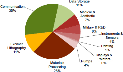
FIGURE 7.8 Review of lasers by application by sales, 2011. SOURCE: Courtesy of Strategies Unlimited and Laser Focus World (2012).
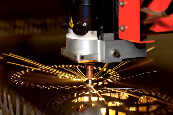
FIGURE 7.9 Laser cutting is used to produce exact components. SOURCE: Image by Bystronic.
processes. Diode-pumped solid-state lasers operating in the near infrared (IR) and excimer lasers operating in the UV to the near IR are most frequently used. Laser selection is a function of a variety of factors, including process scalability, the characteristics of the materials being machined, and operating cost. An important feature of micromachining lasers is their high-pulsed, non-continuous output, with pulse repetition rates that range from a few hertz to several hundred hertz and pulse durations between a few picoseconds and microseconds. The nature of the pulsing aids in the management of the heat load in the material being machined. Figure 7.10 shows slots cut into in stainless steel as small at 75 µm in width.
“Additive manufacturing,” three-dimensional printing, describes a group of technologies that are used to create parts by building up layers to, in effect, “grow a part.” Additive processes are fundamentally different from traditional subtractive processes in which material is removed from a block to create a part. One of the big advantages of additive processes is that the amount of waste material is greatly minimized because only as much source material as is needed is used to build the part. First developed in the mid-1980s, additive manufacturing has grown in acceptance
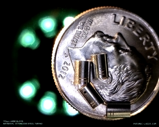
Figure 7.10 Slots cut into stainless steel are 75 µm wide. It should be pointed out that lasers are going to be needed in the future not only for machining but for interferometry for precision manufacturing. Laser interferometry is already being used in IC manufacturing for controlling etching and deposition on a nanometer scale and is going to be even more important in future high-resolution three-dimensional additive manufacturing. SOURCE: Courtesy of Potomac Photonics.
and practice to the point that today it is an effective development and shop floor tool. The improvements in performance and cost-competitiveness associated with additive manufacturing reflect advances in a number of enabling technologies, many of which are based on photonics.
Although not yet a complete replacement for conventional machining or fabrication processes, additive manufacturing has several key advantages. Most notable of the advantages are the short time from computer-aided design (CAD) file to “part complete” and the cost-effectiveness of low-volume production, which reflect the elimination of time to design and produce custom tools or fixtures. Low-volume cost-effectiveness comes from the elimination of high-cost capital tools that would be required to be leveraged over the production of a low number of parts.
Combined advances in three-dimensional design tools, CNC technologies, and lasers have enabled a steady growth in additive-manufacturing capability. Whereas in the past the technology was confined to simple parts for experimental purposes, today complex geometries with a high degree of precision are produced in the laboratory and on the shop floor. The improved capability leveraged with the advantages described earlier makes additive manufacturing a good fit for a class of products that can be produced effectively in the United States. They are prototypes, products with a high degree of customization and complexity, and products produced in low volume.
The following are brief descriptions of a few of the additive-manufacturing processes that illustrate the use of laser technology to produce parts.
In contrast with photolithography, stereolithography is used in larger-scale products. Developed in 1988, it was the first of the rapid prototyping processes. As shown in Figure 7.11, the stereolithographic process deposits layers of approximately 0.002-0.003 in. thick and uses a UV laser to cure the resin only where the
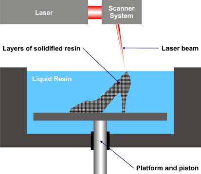
FIGURE 7.11 Stereolithography schematic. SOURCE: Image by Usdabhade.
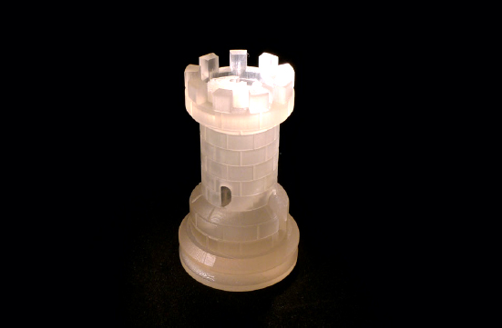
FIGURE 7.12 A stereolithographed chess piece. SOURCE: Courtesy of Potomac Photonics.
material is needed for the part. The laser wavelength and power can vary between manufacturers but is approximately 325 nm from a low-power He-Cd source. The part is built up in layers until the final geometry is completed.
On completion of the layering process, the part is subjected to high-intensity UV light for the postcuring process, which fully hardens the resin. A chess piece fabricated with stereolithography is shown in Figure 7.12.
Selective laser sintering (SLS) was developed in the mid-1980s and is capable of producing parts from thermoplastics, ceramics, or metals. Like stereolithography, SLS, shown in Figure 7.13, is a layering process that builds a part from a powder based on a three-dimensional CAD model. In the SLS process, a laser fuses the layers of powder in localized areas to create the final part geometry. Although systems vary between manufacturers, the laser used is approximately a 50-W CO2 laser. The process can yield very accurate parts with tolerances of ±0.05-0.25 mm. Components fabricated with SLS require no postprocessing. Figure 7.14 shows a replica of a violin produced with the SLS process.
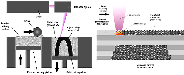
FIGURE 7.13 Selective laser sintering (SLS) schematic. SOURCE: Image by Materialgeeza.

FIGURE 7.14 Martha Cohen, of the Hochschule für Musik und Theater, München, plays a replica of a Stradivarius violin fabricated with SLS during the Kleine Zukunftsmusik der Photonik event. SOURCE: Erik Svedberg, National Research Council.
Laser Engineered Net Shaping (LENS™) was developed in the mid-1990s at the Sandia National Laboratories. The process, shown in Figure 7.15, uses a neodymium-doped yttrium aluminum garnet (Nd:YAG) laser operating at 500-600 W that is enclosed in an argon gas environment. The laser creates a molten pool into which powdered metal is injected. Parts have been produced from stainless-steel alloys, nickel-based alloys, tool-steel alloys, titanium alloys, and other specialty materials, including composites. As in other additive-manufacturing processes, parts originate from three-dimensional CAD models, and material is built up in layers to create the final part. The significant difference between LENS and other additive processes is that the parts obtain the same density as the metal used to fabricate them. Figure 7.16 shows a tool produced with the LENS process.
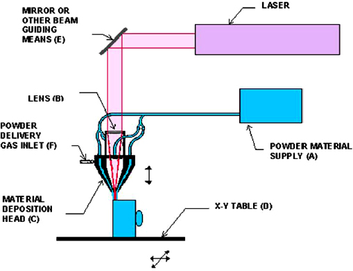
FIGURE 7.15 Laser Engineered Net Shaping (LENS™) process schematic. SOURCE: Worldwide Guide to Rapid Prototyping Website, © Copyright Castle Island Co., all rights reserved. Available at http://www.additive3d.com/len_int.htm. Reprinted with permission.
FIGURE 7.16 H13 tooling created with LENS™ process. SOURCE: Courtesy of Sandia National Laboratories.
A common opportunity exists among these techniques to increase the precision of three-dimensional manufacturing. If shorter-wavelength lasers and imaging were available, it would be possible to reduce the scale of the smallest-possible three-dimensional voxel (a three-dimensional pixel).
In general, one important part of additive manufacturing is an increased emphasis on in situ metrology that uses coherent optics (interference) for feedback and control, especially when the dimensions of parts shrink. Pattern-placement metrology, used ordinarily for lithographic purposes, can rely on phase-coherent fiducial gratings patterned by interference lithography.70 Potential uses include measuring process-induced distortions in substrates, patterning distortions in pattern-mastering systems, and measuring field distortions and alignment errors in steppers and scanners. For example, spatial-phase-locked electron-beam lithography has been implemented to correct pattern-placement errors at the nanometer level.71
_________________
70 Schattenburg, M.L., C. Chen, P.N. Everett, J. Ferrera, P. Konkola, and H.I Smith. 1999. Sub-100 nm metrology using interferometrically produced fiducials. Journal of Vacuum Science and Technology B: Microelectronics and Nanometer Structures 17(6):2692-2697.
71 Hastings, J.T., F. Zhang, and H.I. Smith. 2003. Nanometer-level stitching in raster-scanning electron-beam lithography using spatial-phase locking. Journal of Vacuum Science and Technology B: Microelectronics and Nanometer Structures 21(6):2650-2656.
PHOTONICS AND THE FUTURE OF U.S. MANUFACTURING
As noted earlier, U.S.-based manufacturing now accounts for a smaller share of global manufacturing value added than 20 years ago. The drive for competitiveness and increased shareholder value has caused corporations in nearly every area of photonics to search for alternative manufacturing locations. The exception may be products that have substantial defense-related markets and applications and that therefore are subject to controls over their export (International Traffic in Arms Regulations, ITAR). But government licensing has allowed “offshoring” for some components in this product field as well. During the same period, however, some components continue to be manufactured in the United States and have remained competitive. What distinguishes the components and final assemblies whose production has remained in the United States from those now produced mainly offshore?
A critical factor affecting the location of production is volume. Typically, high-volume production operations are more sensitive to labor and capital cost differentials, and these activities have been among the most likely to move offshore from the United States in photonics and other high-technology products. In photonics, as in other high-technology industries, high-volume production operations are most common in consumer products, and low-volume operations range from the production of test lots to the manufacture of specialized systems.
Advances in optical materials and processing have enabled the manufacture of precision optical components for very low cost with sufficient volume to amortize the required tooling. One example is the mass production of molded polymer aspheres. Their unit costs can be very low as long as the volume is sufficiently high. Low-volume production of these components, however, tends to be expensive because of the large amounts of labor and time required to manufacture and test precision tools. Even when advanced capabilities are used in a highly automated manufacturing process, the cost of the equipment coupled with low volume drives production costs up significantly. Recent advances in several manufacturing capabilities, such as different methods of additive manufacturing, hold out considerable promise for the development of low-cost machines capable of providing precision optics, with surface figures not restricted to the narrow range of surfaces possible with current grinding and finishing techniques. In addition to providing a new set of potential optical surface figures and the associated capabilities, these advances may enable low-cost precision optics even for low-volume applications and thereby remove much of the benefit of moving optics manufacturing overseas by minimizing the impact of labor costs on the optics. Photonics-enabled advances in manufacturing technology thus could slow the erosion, or perhaps support renewed growth, in U.S.-based manufacturing activity.
High-volume products, particularly consumer retail products, generally have cost as a high priority and tend to use manufacturing processes focused on production cost minimization. Manufacturing processes that minimize labor and infrastructure costs are preferred. U.S. manufacturers have, over the years, had difficulty in competing in the high-volume market and have seen much of this work move offshore. That move has been driven in large part by the cost of labor in the United States, which is reflected in raw materials, operations, and overhead. In an effort to compete in at least a portion of the high-volume market (the lower-volume portion of the high-volume market), U.S. manufacturers have used a variety of strategies. For example, manufacturers have changed from commodity components and moved toward precision components and subassemblies in their U.S.-based operations. The high-volume sector tends to be very cost-sensitive, but the lower-volume end of this sector is somewhat less so.
In addition to focusing on products that are less cost-sensitive, manufacturers have reduced the amount of direct labor in their U.S.-based manufacturing processes. In optics grinding and polishing operations, such as lens centering, use of CNC equipment capable of running unattended, as shown in Figure 7.17, has
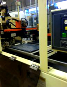
FIGURE 7.17 Automated lens handling. SOURCE: Courtesy of Rochester Precision Optics.
helped to reduce the amount of labor at the component level. In polymer lens molding, the use of automation to remove parts from molds, degate those parts, and the use of molds with higher cavitation, has reduced per part cost and improved competitiveness. Those cost-saving strategies can be capital-intensive, and manufacturers must evaluate the associated economics case by case. The purchase, installation, and maintenance costs of labor-saving equipment must be offset by actual labor savings to justify expenditures.
Low-volume products are generally high-precision and complex or subject to export restrictions linked to national security concerns, as in the case of ITAR. ITAR thus has offsetting effects on the location of innovation and production for U.S. firms. On the one hand, restrictions on export of ITAR-controlled products may lead U.S. firms to site their self-financed product development activities for these products offshore to avoid the restrictions; at least some types of innovation may move offshore from the United States as a result of ITAR. On the other hand, the production of ITAR-controlled products, especially products based on R&D that draw on defense-funded programs or products that are sold in large part to federal agencies, may be less likely to move offshore because of ITAR restrictions on procurement of such products from foreign producers or foreign production sites.
Products not subject to ITAR in the low-volume sector are often in early-stage development and require prototypes or are products in the medical industry, such as complex Lasik surgery equipment. A common characteristic of these products is the requirement for tightly specified precision optical components; emphasis is placed on consistently and reliably satisfying difficult specifications. Although cost is always an important element with all products, it often falls behind the requirement for precision and reliability.
U.S. manufacturers have excelled in the production of low-volume, high-precision optical components and devices. Manufacturers have successfully pushed legacy technologies and adopted newer technologies to satisfy the requirements of this segment. Precision CNC equipment capable of producing components repeatedly and accurately is in wide use. Assembly processes that often require active alignment are used to enable compliance with the requirement for tight tolerances. Complex precision metrology is used for testing components and assemblies to ensure that specifications are met.
THE U.S. MANUFACTURING WORKFORCE
It is the judgment of this committee that advances in photonics provide clear potential for growth in U.S.-based manufacturing by (1) expanding the applications
of photonics throughout manufacturing and thereby improving the cost-competitiveness of processes used to produce high-volume products, (2) accelerating the commercial exploitation of new photonics-based technological opportunities, and (3) improving the cost-competitiveness of U.S. manufacturing of photonics products and components.
Realizing that potential, however, requires a well-trained manufacturing workforce that includes both advanced-degree holders and skilled operators and craftspeople. As was discussed in previous chapters, because of the nature of photonics as a technology rather than an industry on which data are collected by U.S. government statistical agencies, the committee was not able to assemble estimates of current employment in photonics-enabled production activity, nor was it able to forecast growth for various occupations within this sector.72 The collection and reporting of better employment data in photonics will be important for any future federal initiative in this field.
Nonetheless, it is the judgment of the committee that U.S. holders of advanced degrees from university-based programs in photonics, optics, and related disciplines too often pursue careers in R&D or academia rather than pursue opportunities in design or manufacturing within industry. It is important that U.S. firms develop more attractive career paths for advanced-degree holders to pursue careers in photonics manufacturing and in the applications of photonics technologies throughout manufacturing.
Some committee members cited the example of the U.S. semiconductor industry as one that has developed attractive employment opportunities in manufacturing for engineering and science advanced-degree holders. That industry seems to have experienced fewer problems in recruiting top graduates into manufacturing process development, perhaps because leading firms recognize its significance and are willing to make manufacturing jobs attractive by acknowledging that manufacturing is a key ingredient in their competitive advantage.
Similarly, the committee concluded that improvements in technical education are needed to increase the quality of skilled blue-collar workers in optics and photonics. Although U.S. community colleges provide abundant opportunities for students to pursue technical education, there are fewer opportunities for apprenticeship-based training in the U.S. optics industry than in similar industries
_________________
72 Although Chapter 2 presents rough estimates of employment in U.S. firms that are active in photonics, based on their membership in professional or trade organizations, the committee notes in that discussion that such estimates do not represent measures of “photonics-dependent” employment, nor do they enable an analysis of employment prospects or current shortages of skilled workers, scientists, or engineers in photonics-related production or applications. Chapter 4 discusses concerns about the effects of impending retirements and the small pool of U.S. nationals with advanced degrees available for employment in defense-related production and R&D activities, although here, too, precise data on the implications of these trends for photonics applications are lacking.
in Germany. The difficulties of expanding a skilled technical workforce in the United States are considerably exacerbated by the declining performance of U.S. primary and secondary education.73,74 It is, of course, true that weaknesses in the quality and quantity of the skilled blue-collar workforce in the United States can be partially compensated for by expanded investment in automation. But even the intelligent deployment of more highly automated manufacturing processes will be hampered by weaknesses in the skilled workforce in U.S. manufacturing.
Finding: Production of many photonics applications—such as TFT displays, solar modules, and optoelectronic components for communications systems, most of which were first developed and commercialized by U.S. firms in the U.S. economy—now is dominated by foreign production sites, even when these production activities are still controlled by U.S.-based firms. The effects of this offshore movement of manufacturing on innovation in photonics, however, vary considerably among different sectors and technologies within photonics. Indeed, the United States remains the leading source of USPTO patents in two key sectors of photonics (solar and communications components) and is the leader in potential next-generation technologies, such as flexible displays, “paint-on” and other thin-film solar cells, and monolithically integrated optoelectronic devices.
Key Finding: To enable the United States to be productive in manufacturing photonics goods, a capable and fully trained workforce must exist at all levels, including shop floor associates, technicians, and engineers. Because photonics is not yet recognized as an industry and data are not tracked in a way that facilitates analysis, it is difficult to evaluate the extent of personnel shortages in photonics manufacturing and in applications of photonics elsewhere in the manufacturing industry in general. It seems that it would be beneficial if industry and government did more to increase training and employment opportunities in photonics manufacturing.
Key Finding: Additive manufacturing, which uses significant optics and photonics technologies, has become important in manufacturing, and its position is expected to increase. Additive manufacturing tends to require low labor use and is therefore advantageous in regions with high labor costs, such as the United States.
_________________
73 National Research Council. 2010. Standards for K-12 Engineering Education? Washington, D.C.: The National Academies Press.
74 National Research Council. 2011. Successful STEM Education: A Workshop Summary. Washington, D.C.: The National Academies Press.
RECOMMENDATIONS AND GRAND CHALLENGE QUESTION
Key Recommendation: The United States should aggressively develop additive-manufacturing technology and implementation.
Current developments in the area of lower-volume, high-end manufacturing include, for example, three-dimensional printing, also called additive manufacturing. With continued improvements in manufacturing tolerances and surface finish, additive manufacturing has the potential for substantial growth. The technology also has the potential to allow three-dimensional printing near the end user no matter where the design is done.
Key Recommendation: The U.S. government, in concert with industry and academia, should develop soft x-ray light sources and imaging for lithography and three-dimensional manufacturing.
Advances in table-top sources for soft x rays will have a profound impact on lithography and optically based manufacturing. Therefore, investment in these fields should increase to capture intellectual property and maintain a leadership role for these applications. The committee views development of soft x-ray light sources and imaging as an appropriate field for expanded federal R&D funding under the sponsorship of a national photonics initiative undertaken with the advice and financial support of U.S. industry. This chapter indicates the need for an order-of-magnitude or greater increase in resolution in manufacturing.
The above two key recommendations help to inform the fifth and last grand challenge question:
5. How can the U.S. optics and photonics community develop optical sources and imaging tools to support an order of magnitude or more of increased resolution in manufacturing?
Meeting this grand challenge could facilitate a decrease in design rules for lithography, as well as providing the ability to do closed-loop, automated manufacturing of optical elements in three dimensions. Extreme ultraviolet is a challenging technology to develop, but it is needed in order to meet future lithography needs. The next step beyond EUV is to move to soft x rays. Also, the limitations in three-dimensional resolution on laser sintering for three-dimensional manufacturing are based on the wavelength of the lasers used. Shorter wavelengths will move the state of the art to allow more precise additive manufacturing that could eventually lead to three-dimensional printing of optical elements.
Recommendation: Industry and public (both federal and state) sources should expand financial support for the training of skilled workers in photonics production and in applications of photonics-based technologies in manufacturing. The photonics industry also should enhance incentives for holders of advanced degrees in photonics, optics, physics, and related fields to pursue employment opportunities in manufacturing. One potential vehicle for such expanded support and for needed improvements in data collection on photonics employment trends at all levels is the federal initiative in photonics discussed in the recommendations of Chapter 2.


