
4
BEAM APPLICATIONS IN MICROELECTRONICS
Several beam techniques have been incorporated or show promise of applicability in microelectronics manufacture. As a result, this highly competitive industry is one that is most likely to benefit early from the process integration discussed in this report. This chapter reviews important microelectronics applications of beam technologies and outlines uses of these technologies in semiconductor device manufacturing.
BEAM APPLICATIONS IN SEMICONDUCTOR DEVICE MANUFACTURE
Many of the well-developed and widely used applications of beam technologies are in the manufacture of semiconductor devices. The continuous need to produce smaller and more complex structures with higher quality and yield has provided the major emphasis for much of the development of sophisticated beam processes and beam processing equipment. Some of the applications of beam technologies in the fields of integrated circuit and optoelectronics fabrication are reviewed here to illustrate the capabilities and advantages of these technologies over previous manufacturing techniques.
Silicon Integrated Circuits
Although the manufacture of integrated circuits (ICs) is a very precise and complex process, only a few general types of operations are performed. These operations involve deposition, patterning, etching, cleaning, doping by ion implantation, oxidation, diffusion, and heat treatment. A typical sequence of steps is illustrated in Figure 4-1, a sequence performed many times to fabricate a complete circuit. The beam technologies used for the various operations are listed in Table 4-1. Specific examples of some uses of beam technologies are described in the sections that follow.
Beam Technologies For Materials Deposition
Continuous improvement in the speed and functionality of IC has been achieved by a dramatic reduction in the sizes of transistors and interconnection elements. Key to achieving this reduction has been the ability to improve the thickness and compositional uniformity of the metals, dielectrics, and semiconducting materials deposited on the substrate.
Over the past 10 years, sputtering has replaced evaporation as the technology of choice for depositing thin films of metal on IC. Sputtering offers advantages of better control of alloy composition, such as from an Al-Cu-Si alloy target, as well as in situ sputter etching, good thickness uniformity, and superior adhesion. In addition, deposition of refractory metals is generally achieved much better by sputtering than by evaporation.
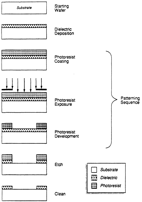
Table 4-1 Beam Applications in Silicon IC Manufacture
|
Deposition Technologies |
|
Material |
Uses |
|
CVD |
|
Si Epitaxy |
Growing controlled layers of semiconductors |
|
|
|
Polysilicon |
Gate electrodes. capacitor plates, interconnects, resistors |
|
|
|
SiO2 |
Insulator. diffusion or implant mask |
|
|
|
Si3N4 |
Insulator, oxidation mask |
|
|
|
W |
Via plugs, interconnects |
|
PACVD |
|
Silicon |
TFTs, resistors, photovoltaics |
|
|
|
SiO2 |
Insulator, diffusion or implant mask |
|
|
|
Si3N4 |
Insulator, oxidation mask, passivation |
|
PVD |
|
Al, Au |
Interconnects |
|
PAPVD |
|
Al, Ti, W |
Interconnects, barriers |
|
|
|
Ni-Cr, SiCrO, TaN |
Resistors |
|
|
|
SiO2 |
Insulator |
|
|
|
Si3N4 |
Insulator |
|
|
|
Silicon |
TFTs, resistors, photovoltaics |
|
Ion beam |
|
B, P, As |
Controlled semiconductor doping |
|
Patterning Technologies |
|
|
Uses (ultimate resolution) |
|
X-ray |
|
|
Masked resist exposure, feature size of |
|
FIB |
|
|
Direct deposition or etching, feature size of |
|
Optical |
|
|
Masked photoresist exposure, feature size of |
|
e-beam |
|
|
Direct write resist exposure, feature size of |
|
Etching Technologies |
Etching Gas |
Material |
Uses |
|
Plasma etching |
C2F6 |
SiO2 |
Diffusion and implant windows, vias |
|
|
CF4/SF4 |
Si3N4 |
Diffusion and oxidation windows |
|
|
CF4/SF6 |
Silicon |
Trench isolation, polysilicon interconnect |
|
|
Cl2/BCl3 |
Aluminum |
Metal interconnect |
|
|
CF4/SF6 |
Tungsten |
Metal interconnect |
|
Plasma etching, |
C2F6 |
SiO2 |
Spacers, planarization |
|
unpatterned |
CF4 |
Si3N4 |
Masking layer removal |
|
|
CF4 |
Polysilicon |
Storage capacitors, three-dimensional structures |
|
|
CF4/SF6 |
Tungsten |
Via plugs |
|
Sputter etching |
Ar |
Any |
Cleaning, surface layer removal |
|
Cleaning Technologies |
|
|
|
|
Sputtering |
Ar |
Any |
Surface cleaning prior to deposition |
|
O2 |
O2 |
Photoresist |
Photoresist removal and surface cleaning |
|
H2 plasma |
H2 |
SiO2 |
Surface cleaning prior to epitaxy |
Low-pressure chemical vapor deposition (LPCVD) is another major technological improvement of the past 10 years. By reducing the deposition pressure to the 1- to 10-Tort range, significant improvements in film quality, cleanliness, and uniformity have been achieved for dielectric and polysilicon depositions. Thickness uniformities of 2 to 3 percent are routinely achieved by batch LPCVD systems. The ability of LPCVD to uniformly and conformally cover very large aspect ratio features has been a major contributor to the ability to manufacture megabit random access memories (RAMs). Selective LPCVD of tungsten shows great promise for improving the reliability of IC interconnections and for increasing their performance (Bertagnolli et al., 1988; Kaanta et al., 1988). Figure 4-2 illustrates interconnect cross-sections with and without tungsten via plugs. An extension of the via-fill method has been used to form a fully planarized refractory metal interconnect scheme (Thomas et al., 1988).
Ion implantation has replaced diffusion for almost all semiconductor doping process steps. It allows controlled impurity profiles and dopant concentrations to better than ±3 percent. The resulting implant doping profiles are not as dependent on temperature and solid solubility as are diffusion doping profiles. Implantation also allows a major reduction of the thermal budget for temperature-sensitive process steps and permits buried-layer profiles, which cannot be readily accomplished with thermal diffusion.
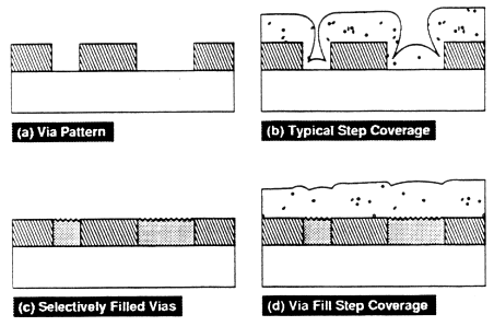
Figure 4-2 Metal step coverage improvement by selective via filling using LPCVD.
Beam Technologies For Patterning
Essentially all of the patterning of silicon ICs is performed by optical lithography, with an optical step-and-repeat lithography sequence being the technology of choice for advanced circuit fabrication. As feature sizes are reduced, the limits of optical lithography will be reached. Electron beam (EB) lithography is used currently in some circuit designs for defining small features and also in some small-volume commercial applications. Because of its high resolution, EB pattern generation is the technology of choice for producing complex optical and x-ray photomasks. Improved EB
capabilities or perhaps use of ion beam writing systems will be required to produce the x-ray masks of the future. Because serial EB is slow, its application to conventional IC production is very limited.
An apparent successor to optical lithography is x-ray lithography. Present research demonstrates that existing x-ray technology can achieve 0.1-µm lithographic features. Although many technical problems remain, the capabilities and costs of production-type x-ray equipment are well enough understood that several industrial and university groups are building or using synchotron x-ray sources to develop IC fabrication processes (Warlaumont, 1989). Electron and ion beams, both focussed and masked, have merit in overcoming some of these lithography problems.
Beam Technologies For Etching
Fine-geometry circuit elements have been made possible by major advances in dry etching. All present methods for dry etching depend on the use of a plasma to generate chemically active radicals in the low-pressure gas ambient. This provides the unique capability to etch highly anisotropically, which allows preparation of much smaller feature dimensions and gives the ability to create three-dimensional structures. The combination of LPCVD deposition and anisotropic etching has led to recent increases in dynamic RAM (DRAM) density (Ema et al., 1988; Shen et al., 1989). The anisotropic capability of dry etching also allows fabrication of several key features in IC circuits, as shown in Figures 4-3 through Figure 4-5.
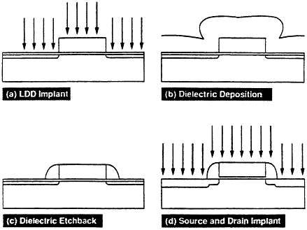
Figure 4-3 Schematic of a spacer-protected metal-oxide semiconductor (MOS) transistor formation.
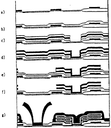
Figure 4-4 Schematic of a stacked ''fin'' capacitor formation process. (a) transister formation; (b) SiN deposition; (c) SiO2, polysilicon, SIO2 deposition; and contact hole formation; (d) polysilicon; (e) storage electrode patterning; (f) SiO2 removal by hydrofluoric acid solution; (g) capacitor film growth, polysilicon deposition, cell plate, and bit line formation. No extra mask process is necessary to form fin structure; the number of fins can be easily changed.
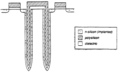
Figure 4-5 Schematic trench-capacitor cell structure.
BEAM TECHNOLOGIES FOR COMPOUND SEMICONDUCTOR ICs
Most of the processing technologies used for compound semiconductor IC fabrication are identical to those used for silicon ICs. Newer device structures, such as heterojunction field effect transistors (HFETs) and heterojunction bipolar transistors (HBTs), depend heavily on metal-organic chemical vapor deposition (MOCVD) and MBE beam technologies to create highly uniform, precisely controlled epitaxial layers of different materials (Asbeck et al., 1987; Ng et al., 1989). Table 4-2 describes additional beam technologies that are applied to the fabrication of compound semiconductor Ics.
Table 4-2 Beam Applications for Compound Semiconductor IC Processing
|
Deposition Technologies |
|
Material |
Uses |
|
MOCVD |
|
GaAs |
Buffer layers, FET channels |
|
MBE |
|
AlGaAs |
Super lattice buffers, heterojunction transistors |
|
|
|
InGaAs |
Heterojunction transistors, contacts |
|
|
|
InAlAs |
Heterojunction transistors, contacts |
|
Etching Technologies |
Etching Gas |
Material |
Uses |
|
Plasma etching |
Cl2 |
GaAs |
Selective material removal, backside vias |
|
Ion milling |
Ar |
Gold |
Interconnect etching |
|
Heating |
Ambient |
|
Uses |
|
Rapid optical anneal |
Ar, AsH3, N2 |
|
Implant activation, contact formation |
Beam Technologies For Materials Deposition
The two highly precise growth technologies, developed to prepare epitaxial layers of compound semiconductor with the extremely precise control of stoichiometry, doping, and thickness required for high-performance devices, are MBE and MOCVD. Figure 4-6 shows two of these complex structures.
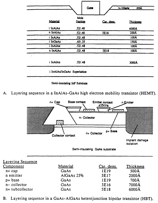
Figure 4-6 Illustration of complex transistor structures.
Beam Technologies For Heating
The abrupt interfaces and bandgap engineering necessary to produce heterostructure devices must be preserved during device processing. Prolonged high-temperature annealing will cause layer mixing and loss of interface abruptness. To minimize these problems, rapid thermal annealing is often used to activate the implants of heterostructure devices. Heat-up and cool-down times of a few seconds are accomplished by optical heating of the substrate with large banks of high-intensity lamps. The same technique is often applied to form ohmic contacts to GaAs and to Si ICs when the thermal budget is tight.
OPTOELECTRONICS
Processing techniques to fabricate optoelectronic components are similar to those used to fabricate heterojunction compound semiconductor devices. GaAs-AIGaAs heterojunction layers have been in use for over 20 years. In the past most such devices were fabricated by liquid-phase epitaxy or chloride-transport vapor-phase epitaxy. Today, MBE and MOCVD techniques provide the capability to fabricate higher-performance yet more complex devices that use superlattices and quantum-well confinement. These may contain integrated devices employing both GaAs and InP semiconductors.
REFERENCES
Asbeck, E. M., M. F. Chang, K. C. Wang, D. L. Miller, G. J. Sullivan, N. H. Sheng, E. Soveno, and J. A. Higgins. 1987. Heterojunction Bipolar Transistors for Microwave and Millimeter-Wave Integrated Circuits. IEEE Transactions on Electron Devices (ED-34), 12Dec.:2571-2579.
Bertagnolli, E., C. Wieczorek, J. Berthold, W. Rosner, B. Hoffman, and H. Schaber. 1988. Low Resistance Via Hole Filling by Blanket W-CVD. Proceedings of the Fifth International IEEE VLSI Multilevel Interconnect Conference, pp. 324-330. IEEE, New York.
Ema, T., S. Kawanago, T. Nishi, S. Yoshida, H. Nishibe, T. Yubu, Y. Kodama, T. Nakano, and M. Taguchi. 1988. 3-Dimensional Stacked Capacitor Cell for 16M and 64M DRAMS. International Electron Devices Meeting Technical Digest, pp. 592-595. IEEE, New York.
Kaanta, C., W. Cote, J. Cuoninik-Holland, P. Lee, and T. Wright. 1988. Submicron Wiring Technology with Tungsten Planarization. Proceedings of the Fifth International IEEE VLSI Multilevel Interconnect Conference, pp. 21-28. IEEE, New York.
Ng, G., D. Pavlidis, M. Tutt, J. E. Oh, P. K. Battacharya. 1989. Improved Strained HEMT Characteristics Using Double-Heterojunction in .65Ga .35As/In .52Al .48As Design. IEEE Electron Devices Letters 10(3):114-116.
Shen, B., G. Chung, I. Chen, D. Coleman, P. Ying, R. McKee, M. Yashino, and C. Teng. 1989. Scalability of a Trench Capacitor Cell for 64 MBIT DRAM. International Electron Devices Meeting Technical Digest, pp. 27-30. IEEE, New York.
Stinton, D. P., T. M. Besmann, and R. A. Lowden. 1988. Advanced Ceramics by Chemical Vapor Deposition Techniques. American Ceramic Society Bulletin 67(2):350.
Thomas, D. C., S. S. Wong, D. R. Dinsmore, and R. J. Soave. 1988. A Multilevel Tungsten Interconnect Technology. International Electron Devices Meeting Technical Digest, pp. 466-469. IEEE, New York.
Warlaumont, J. 1989. X-ray Lithography: On the Path to Manufacturing. Journal of Vacuum Science and Technology. [B]7(6):1634-1641.


