
Fabrication Technology and the Challenges of Large-Scale Production
Karen W. Markus
MCNC
Research Triangle Park, North Carolina
As the commercial and military implementation of microelectromechanical systems (MEMS) technology solutions moves further up the line from research to consumer and commodity applications, the need for a robust manufacturing technology base for MEMS continues to increase. MEMS, the merging of computation with sensing and actuation into an integrated system-based solution for problems pertaining to the physical world, has benefited greatly and grown rapidly out of the widespread manufacturing infrastructure existing in the United States. The U.S. approach to MEMS involves applying the repetitive-layering, batch-processed wafer methods of the integrated silicon circuit manufacturing industry (the IC industry) in order to achieve revolutionary strides in mechanical miniaturization and system integration (Figure 1). This outgrowth from the IC industry has both benefits and pitfalls; capitalizing on the benefits and navigating the pitfalls will determine our success in moving from current low or sporadic MEMS volumes to high-volume successes demanding large-scale production capabilities.
One of the many benefits MEMS technology derives from its common base with the IC industry is the methodology behind its fabrication sequences. Most MEMS processes can be decomposed into a repeating series of material deposition, patterning, and subsequent removal of specific areas of the material. This layering is repeated until the basic structure is created either on or within the silicon wafer. However, although many of these steps, or unit processes, are similar to those used in IC processing, the mechanical nature of MEMS puts additional stringent requirements on the processes. Beyond the fabrication of the basic wafer structure, the releasing of the structures, the handling of these released wafers or die, the packaging, and the testing of the
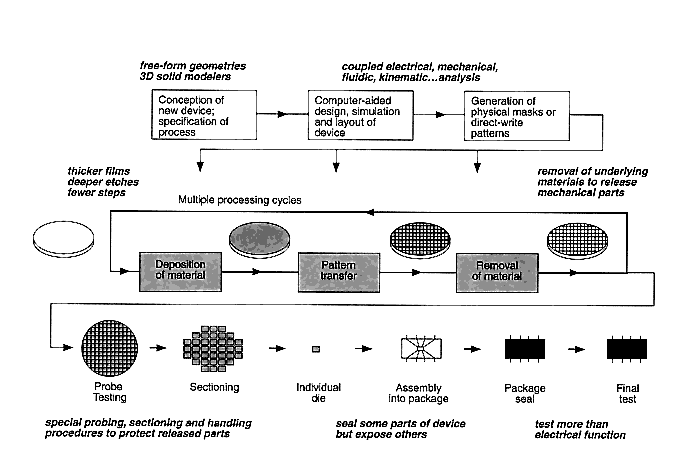
MEMS devices all can challenge even the most sophisticated and technically advanced manufacturing line.
Examples of some of the areas in which MEMS processing differences continue to challenge the norms established by both the IC fabricators and equipment manufacturers include the following.
Design Aids
Creation of new ICs normally entails employing fully integrated computer-aided design tools, from creation through completion. For MEMS, however, these tools are just beginning to be developed for commercial activities, and they exist as discrete, stand-alone programs relevant to only a small piece of the design-simulate-fabricate-validate cycle. One of the most challenging aspects of CAD for MEMS is the multidomain nature of the devices. Whereas electronic circuits function almost exclusively in the electrical domain, MEMS device operation transcends boundaries among thermal, fluid, electrical, mechanical, magnetic, and optical domains. MEMS' need for coupled solutions over several domains challenges the state of the art in CAD.
Lithography
Whereas ICs are pushing the limits of optical lithography down below 0.35 m, MEMS are pushing the same equipment base not to smaller feature size but rather to greater depth of focus. Typical surface micromachined MEMS devices can exhibit 8 microns of topography by the end of the process, compared with 0.5–1.0 micron for advanced IC processes.
Etching
This topography generally is created using thicker deposited materials that serve as the active mechanical layers. Once they are patterned lithographically, these thick layers must undergo robust etch processes that have the capability to etch through the layers selectively and anisotropically while still maintaining critical line size dimensions and edge profiles.
Parametric Testing
A production IC process is monitored by a regular, well-characterized set of parametric test structures. These structures are designed both to screen the health of the integrated process during fabrication and to act as a prefunctional testing screen. Such a set of parametric test structures is yet to be developed, characterized, and implemented in most of the critical MEMS processes. Although many of the basic resistance, capacitance, and defect density test struc-
tures utilized in IC processing can be used, the mechanical nature of the materials for MEMS provides a challenge to the MEMS process engineer attempting to monitor the outcome of the fabrication run. How does one nondestructively measure, monitor, and characterize Young's modulus, residual stress (including gradients), Poisson's ratio, and other material parameters of a deposited film that is intimately affected by both the processing and testing conditions? Does one stack several of these layers together and monitor them?
Functional Testing
Functional testing of ICs generally is performed at the wafer level, and sometimes again after packaging, and is achieved mostly through the use of high-speed electronic testers capable of producing an input voltage (generally 5V or less) or current and then measuring the state of various output nodes. The driving forces in IC testing have been both the number of electrical inputs and outputs necessary to operate the chip (pin count) and the speed of operation. For MEMS testing, the pin count tends to be extremely low: a few to a few tens of pins. Voltages, however, can range into the hundreds of volts for some actuators. Additionally, with the exception of such notables as the Analog Devices ADXL-50 and the Texas Instruments Digital Light Processors (DLP), most MEMS devices produced today have little if any electronics integrally processed with the mechanical devices. This means that the tester must provide the necessary control and feedback functions as well. Similarly, if the device function is to sense a fluid or chemical presence, a severe ''shock," or an optical signal, full functional testing of these devices requires the presence of the appropriate environmental factor.
Packaging
Currently, packaging is the Achilles' heel of MEMS manufacturing. Unlike IC packaging, MEMS packaging is an application-specific task and can completely destroy a potential product's ability to reach the marketplace. Generic methodologies for the packaging of classes of MEMS structures currently do not exist, but they are essential to the continued growth of the field. Every company, large or small, that enters the field cannot afford to travel the long route of learning that some of the early MEMS product pioneers have had to traverse. MEMS packages must have the ability to meet at least one or more of the following criteria:
- isolate nonsensing areas from sensing areas, often in harsh, corrosive, or mechanically demanding environments;
- not impede mechanical action, such as tilting, twisting, rotating, sliding, or vibrating;
- allow the transfer of fluids from one region to another;
- allow the coupling of energy, motion, or momentum from one region to another; and
- not transfer mechanical strain, heat, pressure, moisture, outgassing, performance restriction, and so on to the part in the package.
Equipment
A great majority of those companies currently involved in MEMS fabrication are performing their processing in facilities previously outfitted for IC processing and on equipment that the fast-growing IC industry has outgrown. The extremely large wafer sizes and cutting-edge lithography processes that are the norm in the IC industry currently are not required for MEMS, which allows MEMS fabricators to capitalize their facilities at a fraction of the cost of the newest IC fabs by using "last-year's" refurbished equipment. The down side to this is the limited influence that the MEMS technologists have on the semiconductor processing equipment manufacturers in urging them to develop innovative manufacturing solutions.
The movement of MEMS technology from its current position of "little sister" of the IC industry to dominant force in system manufacturing will require considerable effort on the part of MEMS manufacturers to overcome the impediments to large-scale manufacturing. The closer the MEMS process is to that of the IC process, the easier this transition will be. An example is the Analog Devices (ADI) surface micromachined accelerometer. This MEMS device, rather than being more different, has more in common with the IC technology from which it evolved. For ADI the transition from pilot-line project to major commodity product has been a well-defined path, with reasonable levels of support from existing manufacturing infrastructure.
In contrast are the long growth and development cycles experienced by manufacturers of bulk silicon micromachined devices, which share far less of their processing sequence with ICs than surface micromachining. Although bulk micromachined products have been successful in the marketplace for processing generations longer than surface micromachining, there has been little advance in the state of the art for bulk micromachining. Only recently has advanced reactive ion etching technology been introduced, which will enhance the yield, design, and performance of bulk devices, and this is because this technology is an offshoot of the DRAM market's trench etching requirements. Lithography equipment capable of supporting enhanced two-sided alignment and multiple-wafer aligned bonding has been developed only recently.
These basic perturbations on silicon IC manufacturing technology both enable the field and threaten to hold it back. Silicon IC technology evolved from specialized high-cost tools to low-cost consumer products (smart toast-
ers!?) as a result of the drive exerted by advanced large-scale manufacturing. MEMS technology has received a considerable leg up from the manufacturing equipment, testing, and process engineering technology base established by the domestic IC industry. But unless the key differences and challenges that drive MEMS are adequately addressed and supported through both innovation and manufacturing resources, MEMS will be relegated to a position of "niche market item" rather than the enabling, revolutionary technology toward which it is evolving.


