
Appendix F
Sample Fabrication Sequence for a Standard Printed Circuit Board
The following sequence of steps helps convey the complexity of the process of fabricating a standard printed circuit board.
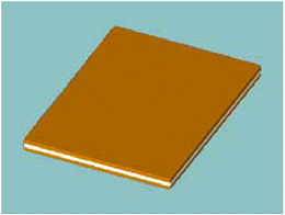
Purchased Copper Clad Dielectric
-
Copper clad is measured in ounces, which converts to inches of thickness (1 oz is ~0.0014 in. thick).
-
Clad may be on one or both sides of dielectric.
-
Dielectric materials are determined by the design requirement. Common materials are glass-reinforced epoxies, glass-reinforced polyimides, polyimide films, and PTFE (Teflon).
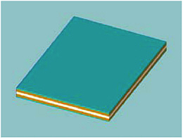
Preparation of the Copper Surface
-
Cleaning can be done mechanically or chemically.
-
Photoresist is a coating of photosensitive material to be used to place the image of the inner-layer circuit pattern on the clad material.
|
|
NOTE: The figures and text in this appendix are drawn from educational materials available at http://www.rockwellcollins.com/about/additionalproducts/collinsprintedcircuits/making_circuit_boards/index.html and are used by permission from Rockwell Collins, Cedar Rapids, Iowa. |
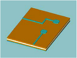
Photo Process
-
Expose is the photo process of transferring the circuit image, which is on working tools, to the copper surface. The photo light causes the resist to harden (polymerize) and to be retained during the subsequent process steps.
-
Develop chemically removes the remaining resist that was not exposed to the light source, as defined by the tooling.
Inner Circuitry
-
Etch is the chemical process that removes the unwanted copper in order to define the circuit image.
-
The etch process will not attack the copper protected by the photoresist.
-
Some amount under the resist may etch, thus causing the cross-section view of the circuitry to have an hourglass appearance.
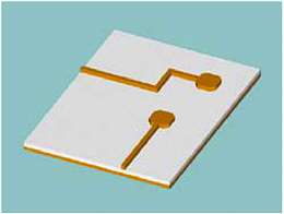
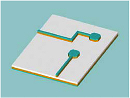
Inner Circuitry
-
Strip is a chemical process that washes off the remaining photoresist leaving the circuit pattern in copper.
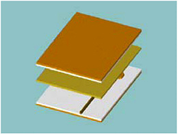
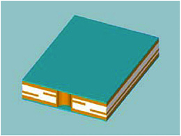
Bond Package
-
Layup is the procedure by which a multilayer package is assembled. The circuit layers (laminates) are stacked over pins in plates, in numerical circuit order. Between each laminate is placed a predefined thickness of bonding material, usually a multiple of sheets.

Bonding
-
The lamination process is a temperature and pressure method, typically performed under vacuum.
-
During lamination the resin in the bond material liquefies and then cures back to a solid state creating a homogenous package.
-
Although different bonding and laminate materials may be interchanged, the best results are usually found when using common dielectrics that are compatible.
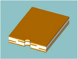
Interconnection
-
Drilling of holes using the design data for size and location is the start of the interconnect process. Drilling provides the mechanical opening that contacts or clears internal features. In the case of many internal layers (multilayer), the contact points are now the avenue of electrical communication.
-
Hole clean is the process (usually chemical) that removes any internal debris from the internal connection. Depending on the materials and specifications, the walls can be simply cleaned (desmear) or aggressively attacked (etchback).
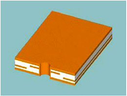
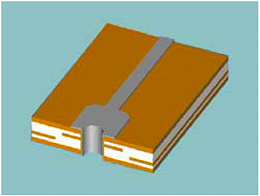
Plated Connection
-
Cleaning and activating solutions prepare the internal hole surfaces for copper plating.
-
Electroless copper chemically plates an initial thin copper layer over the whole panel surface. This provides a surface that can now be electrically plated, which will provide a thicker amount of copper to build a tublet-type hole.
-
Strike plate is the electroplate process that deposits additional amounts of copper in the holes and on the surface. (This process is optional.)
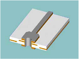
Preparation for Outer Features
-
This step is similar to the inner process of surface preparation, except that here the plan is to define the outer features. The clean and photoresist application steps are very similar.
-
The coating process can be used with varying thicknesses of resists to allow for specific photo and plating process operations. The resist thickness is usually greater when multiple, subsequent plating steps are involved.
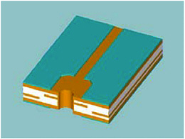
Photo Process
-
The steps in this process are similar to those for the inner process. The expose process, although similar, has the basic concept reversed. The photo tooling has been made to allow the polymerized areas to be where copper will be later removed.
-
Develop will chemically remove the resist on the surface features, opening a pocket for additional plating and revealing the prior plated copper.
Surface Finish
-
Pattern plate means the plating of defined features. It is the process by which additional copper is electrically deposited in the developed cavities.
-
This final copper plate will bring hole sizes and surface-feature thicknesses up to customer specifications.
-
This copper-plated surface is then overplated, normally with a type of tin-lead; nickel or gold are also used as specified by design.
Outer Circuitry
-
The etch chemical process now removes all of the unwanted copper as supplied by the raw material vendor and plated on at electroless and strike (panel) operations.
-
Similar to the inner etch, a surface cross-section view of the circuitries will show hourglassing.
-
At this point in the build process the design is electrically completed.
-
The only steps remaining are those of finishing the surface requirements, creating the mechanical size features, and the final inspecting.
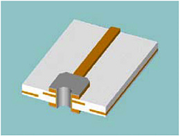
Photo Expose and Strip Tin-Lead
-
The tin-lead strip process involves cleaning the panel, laminating the photoresist on the panel, exposing and developing a pattern to selectively strip the tin-lead. This prepares the copper lines for soldermask to become the protective coating over the bare copper lines.
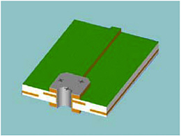
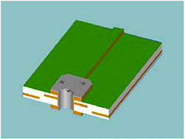
Liquid Photo-Imageable Soldermask
-
Soldermask is a protective layer of acrylic-epoxy (normally green) applied over bare copper lines. The process is known as solder mask over bare copper (SMOBC). The process for applying soldermask is clean, coat, expose, develop, and cure.
Solderable Finishes
-
The earliest final finish was reflowed tin-lead, in which tin-lead etch resist was melted using hot oil to form a solderable finish.
-
Next came solder coating using a process called hot air solder leveling (HASL), in which boards are dipped in molten solder and withdrawn through forced air, which leveled the solder coating.
-
Lately, immersion finishes have gained favor owing to the planar deposit they provide. Planar deposits help placement and soldering of tiny components.
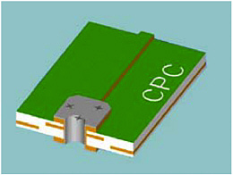
Identification
-
A silkscreen legend is either a customer requirement for component identification, or it is completed by the printed circuit board supplier and used for board identification.
-
Colors of ink are normally black, white, yellow, or red.


